PHYS 351 · Lecture 04 01
Lecture 04
Field-Effect Transistors and Motor Control Covers Lab 4
© Ran Yang, Ph.D. Advanced Instrumentation
PHYS 351 · Lecture 04 02
Today, in one line Separate the signal path from the power path .
The pin decides when . A transistor and its own supply decide how much .
They meet only at the gate, and at a shared ground.
© Ran Yang, Ph.D. Advanced Instrumentation
PHYS 351 · Lecture 04 03
Three acts 1. How a transistor works. Doping, the BJT, then the field effect.
Why a FET is not just a smaller relay.
2. The MOSFET as a switch. On resistance, gate drive, logic level.
3. Driving the motor. Flyback, grounding, and measuring what you built.
Act 1 is what Lab 4 assumes you already have. It is worth the twenty minutes.
© Ran Yang, Ph.D. Advanced Instrumentation
PHYS 351 · Lecture 04 04
Where each task points Task You do Idea 1 PWM on BCM 12; find where it stays valid; screenshots software PWM limits 2 IRL510 datasheet; pinout; motor on a + 5 +5 + 5 MOSFET switch, flyback, ground 3 gate from BCM 12; vary the speed logic-level gate drive 4 rotation-rate detector; duty vs RPM, 10+ points; fit; accuracy optical tachometer
PWM from Lab 3, the photodiode from Lab 1. New this week: the MOSFET in between.
© Ran Yang, Ph.D. Advanced Instrumentation
PHYS 351 · Lecture 04 05
PWM revisited
© Ran Yang, Ph.D. Advanced Instrumentation
PHYS 351 · Lecture 04 06
Task 1 is a characterisation, not a demo “Functions as expected” needs a definition. Write it down first:
measured frequency within, say, 5 % of commanded measured duty within a stated tolerance clean 0 to 3.3 V transitions jitter small compared with the period The answer is a region on a frequency–duty map, not one number.
© Ran Yang, Ph.D. Advanced Instrumentation
PHYS 351 · Lecture 04 07
Where software PWM breaks Region What you see below a few Hz electrically fine; the motor gets kicks, not an average mid-band frequency and duty both track: use this for the motor high frequency f f f near 0 % or 100 % the narrow pulse stretches or vanishes
Sweep a grid: 5–6 frequencies; at each, duty ≈ \approx ≈
© Ran Yang, Ph.D. Advanced Instrumentation
PHYS 351 · Lecture 04 08
Try it At 1 kHz, what on-time is a 2 % duty cycle? At 20 Hz?
If an edge lands only to within 150 μ \upmu μ
© Ran Yang, Ph.D. Advanced Instrumentation
PHYS 351 · Lecture 04 09
Why a pin cannot drive a motor
© Ran Yang, Ph.D. Advanced Instrumentation
PHYS 351 · Lecture 04 10
Three independent reasons Current. 16 mA per pin. A small motor: hundreds of mA, more at stall.
I stall = V supply / R winding I_{\text{stall}} = V_{\text{supply}} / R_{\text{winding}} I stall = V supply / R winding Inductance. Interrupt the current and the winding fights back: V L = − L d I / d t V_L = -L\,\mathrm{d}I/\mathrm{d}t V L = − L d I / d t
Back-EMF. A spinning motor is a generator, V back = k e ω V_{\text{back}} = k_e\,\omega V back = k e ω
© Ran Yang, Ph.D. Advanced Instrumentation
PHYS 351 · Lecture 04 11
So put something in between You need a part that takes a tiny command from the pin and lets through
amperes from another supply.
That part is a transistor. Which kind, and why that kind, is the next twenty minutes.
© Ran Yang, Ph.D. Advanced Instrumentation
PHYS 351 · Lecture 04 12
Act 1 | How a transistor works
© Ran Yang, Ph.D. Advanced Instrumentation
PHYS 351 · Lecture 04 13
Rewind: pure silicon does almost nothing Silicon has four valence electrons and shares all four in the crystal.
Nothing is free to move.
Thermal energy frees the occasional electron, leaving a hole behind.
That is an intrinsic semiconductor: a poor conductor and a poor insulator.
Useful devices start by deliberately spoiling this perfect crystal.
© Ran Yang, Ph.D. Advanced Instrumentation
PHYS 351 · Lecture 04 14
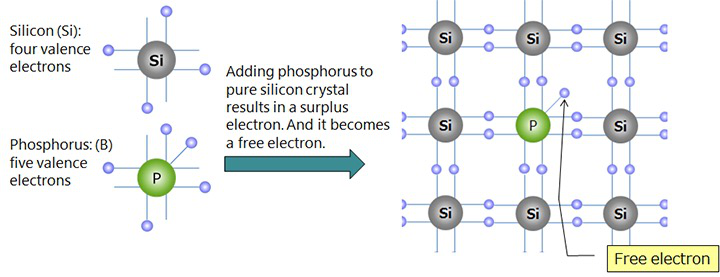
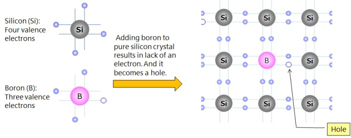
Rewind: doping makes carriers n-type : a spare electron
p-type : a spare hole
Five valence electrons (phosphorus) leaves one over. Three (boron) leaves one missing.
© Ran Yang, Ph.D. Advanced Instrumentation
PHYS 351 · Lecture 04 15
Rewind: join them and you get a diode At the junction electrons cross and fill holes. What is left is a
depletion layer : no free carriers, and a built-in barrier.
Forward bias pushes carriers in and the barrier collapses at about 0.7 V.
Reverse bias widens the depletion layer and nothing flows.
Remember the width of that layer. The JFET is about to control it on purpose.
© Ran Yang, Ph.D. Advanced Instrumentation
PHYS 351 · Lecture 04 16
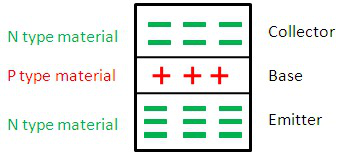
The BJT: two junctions, three regions Emitter heavily doped, base lightly doped and thin , collector in between.
Base–emitter forward biased, base–collector reverse biased.
Carriers injected into the thin base mostly shoot through to the collector.
© Ran Yang, Ph.D. Advanced Instrumentation
PHYS 351 · Lecture 04 17
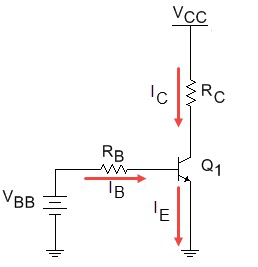
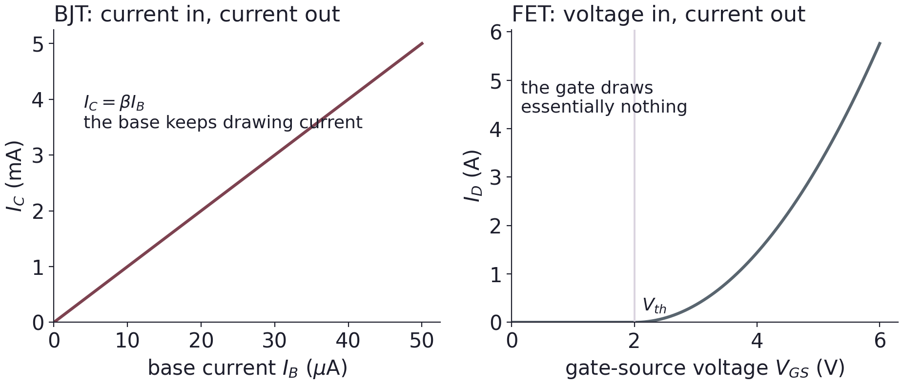
The BJT is controlled by current I C = β I B I_C = \beta\,I_B I C = β I B The base current is not a one-off. It flows the whole time the device is
on, and β \beta β
To hold 1 A at β = 50 \beta = 50 β = 50
© Ran Yang, Ph.D. Advanced Instrumentation
PHYS 351 · Lecture 04 18
The field effect
© Ran Yang, Ph.D. Advanced Instrumentation
PHYS 351 · Lecture 04 19
A different idea: control with a field Instead of injecting carriers, use the electric field from a nearby electrode to
change how many carriers the channel already has.
A field costs no steady current to maintain. That sentence is why your
3.3 V pin can command amperes.
© Ran Yang, Ph.D. Advanced Instrumentation
PHYS 351 · Lecture 04 20
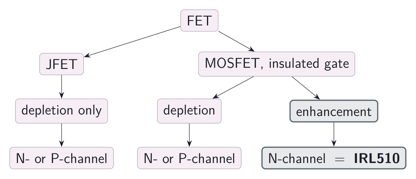
The FET family Every FET has the same three terminals: gate, drain, source.
© Ran Yang, Ph.D. Advanced Instrumentation
PHYS 351 · Lecture 04 21
Channel and gate The channel is the path from drain to source.
The gate decides how much of it conducts.
Current flows drain to source; the gate only sets the valve position.
Two ways to build that valve: pinch an existing channel, or create one. JFET and MOSFET.
© Ran Yang, Ph.D. Advanced Instrumentation
PHYS 351 · Lecture 04 22
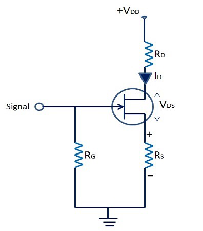
JFET: normally on, squeeze it shut The channel is already there, so a JFET conducts at V G S = 0 V_{GS} = 0 V GS = 0
Reverse bias the gate and its depletion region grows into the channel until it
pinches off.
Never forward bias the gate.
A voltage-controlled resistor, as used in mixers.
© Ran Yang, Ph.D. Advanced Instrumentation
PHYS 351 · Lecture 04 23
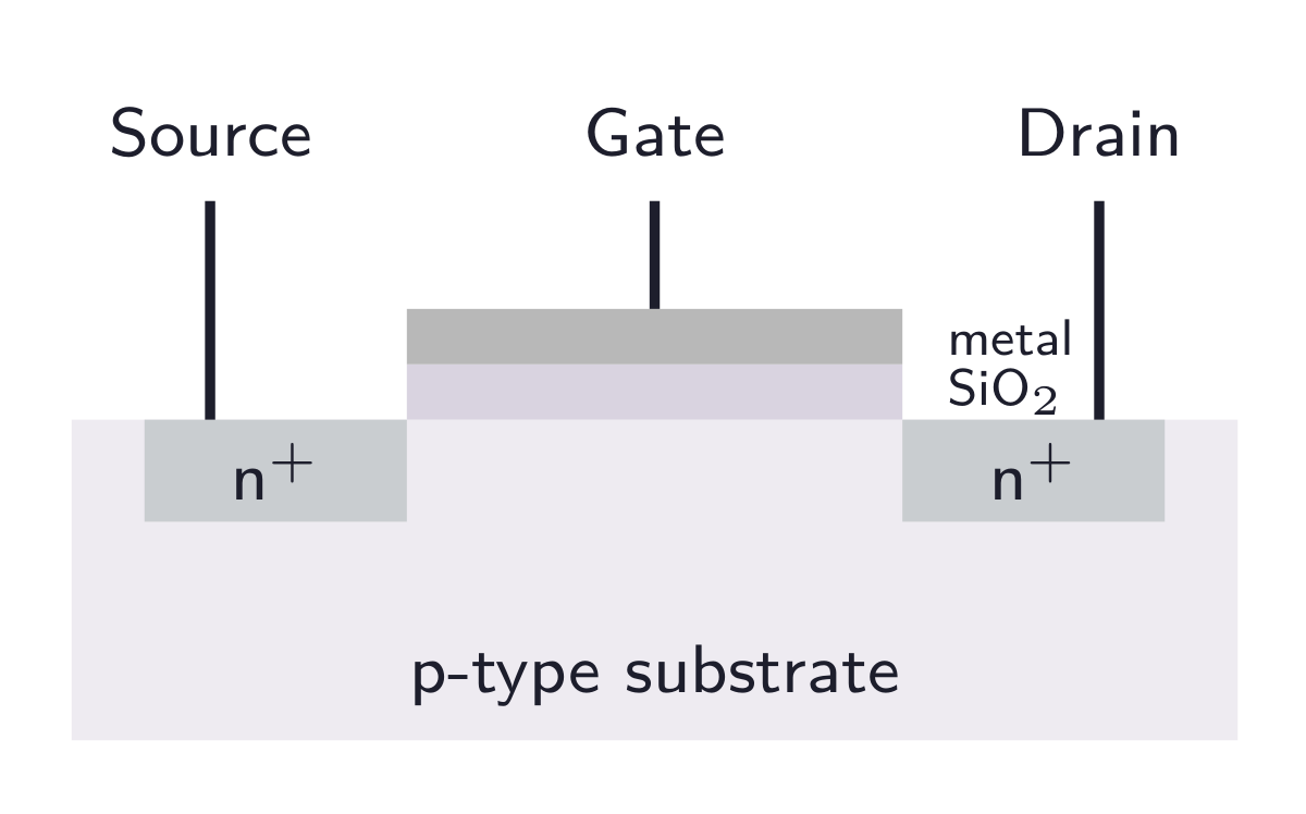
MOSFET: put glass under the gate The gate sits on a thin SiO2 _2 2 layer, so it is no longer a diode. It is a
capacitor . At V G S = 0 V_{GS} = 0 V GS = 0 + ^+ +
© Ran Yang, Ph.D. Advanced Instrumentation
PHYS 351 · Lecture 04 24
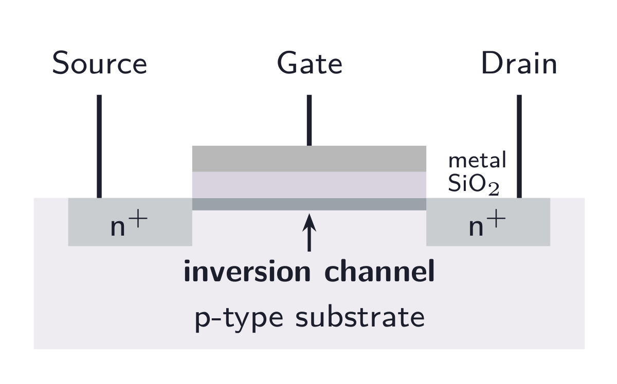
Enhancement: the field builds the channel Raise V G S V_{GS} V GS inversion layer bridges the wells. Above V t h V_{th} V t h
© Ran Yang, Ph.D. Advanced Instrumentation
PHYS 351 · Lecture 04 25
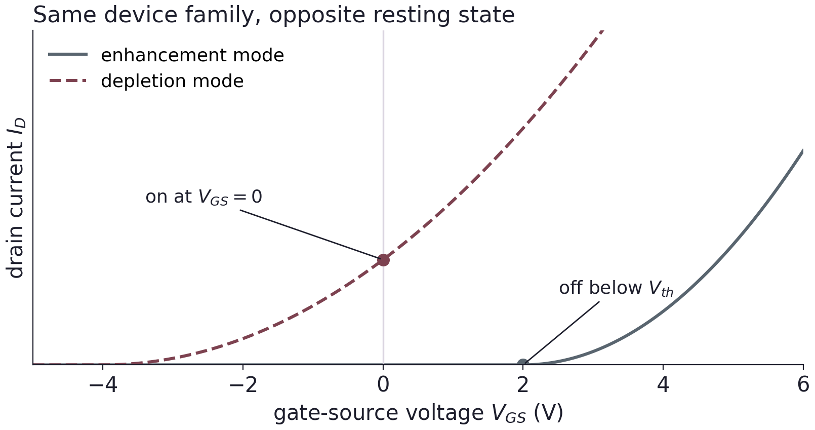
Two modes, one table V G S < 0 V_{GS} < 0 V GS < 0 V G S = 0 V_{GS} = 0 V GS = 0 V G S > 0 V_{GS} > 0 V GS > 0 Depletion mode channel off channel on channel on Enhancement mode — channel off channel on
A depletion device is normally on . An enhancement device is normally off .
For a switch you want normally off, so a loose wire leaves the motor stopped. Enhancement.
© Ran Yang, Ph.D. Advanced Instrumentation
PHYS 351 · Lecture 04 26
The same thing as a curve Shapes, not datasheet values. What matters is where each curve leaves the axis.
© Ran Yang, Ph.D. Advanced Instrumentation
PHYS 351 · Lecture 04 27
FET against BJT BJT FET Controlled by base current gate voltage Control draws current, continuously nothing, after the switching edge Input impedance moderate extremely high, an oxide Carriers electrons and holes one kind only Fully on looks like a residual V C E ( sat ) ≈ 0.2 V_{CE(\text{sat})} \approx 0.2 V C E ( sat ) ≈ 0.2 a resistance R D S ( o n ) \Rds R DS ( on ) Loss at 1 A ≈ 0.2 \approx 0.2 ≈ 0.2 I 2 R D S ( o n ) I^2\Rds I 2 R DS ( on ) R D S ( o n ) \Rds R DS ( on ) Drive from logic needs a base resistor and current connect the pin, with a gate resistor Killed by heat, overcurrent static , over-voltage on the gate
For a logic-driven power switch the FET wins on all three.
© Ran Yang, Ph.D. Advanced Instrumentation
PHYS 351 · Lecture 04 28
Why that comparison decides Lab 4 A BJT wants tens of mA of base current, for as long as the motor runs.
Your pin has 16 mA in total .
The FET asks only for a brief charging pulse.
© Ran Yang, Ph.D. Advanced Instrumentation
PHYS 351 · Lecture 04 29
The gate is fragile, and that is the trade The oxide is a few tens of atoms thick. It buys you the free gate drive, and it is
also what static discharge punctures.
Handle the part by its package. Never let the gate float.
Respect V G S , max V_{GS,\max} V GS , m a x ± 20 \pm 20 ± 20
A dead MOSFET usually died at the gate, not the drain.
© Ran Yang, Ph.D. Advanced Instrumentation
PHYS 351 · Lecture 04 30
Act 2 | The MOSFET as a switch
© Ran Yang, Ph.D. Advanced Instrumentation
PHYS 351 · Lecture 04 31
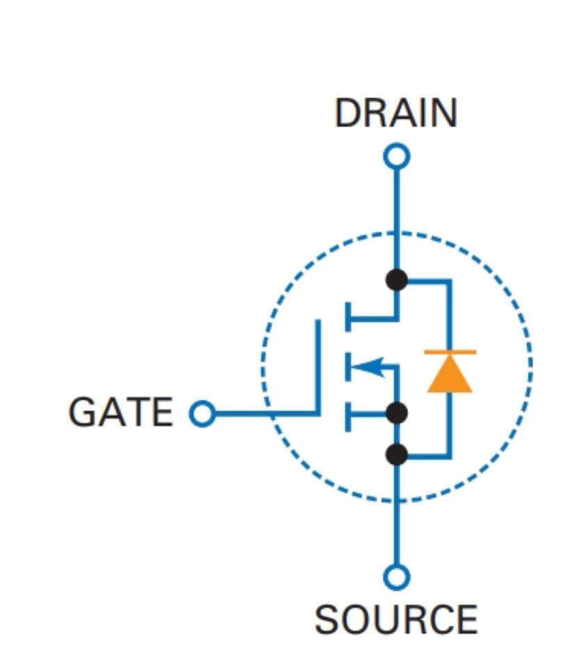
The symbol, and the diode you did not ask for Gate, drain, source, and an anti-parallel body diode that comes free with
the structure.
It points the right way to catch an inductive kick.
Free, but slower and weaker than a real flyback diode. Fit your own.
© Ran Yang, Ph.D. Advanced Instrumentation
PHYS 351 · Lecture 04 32
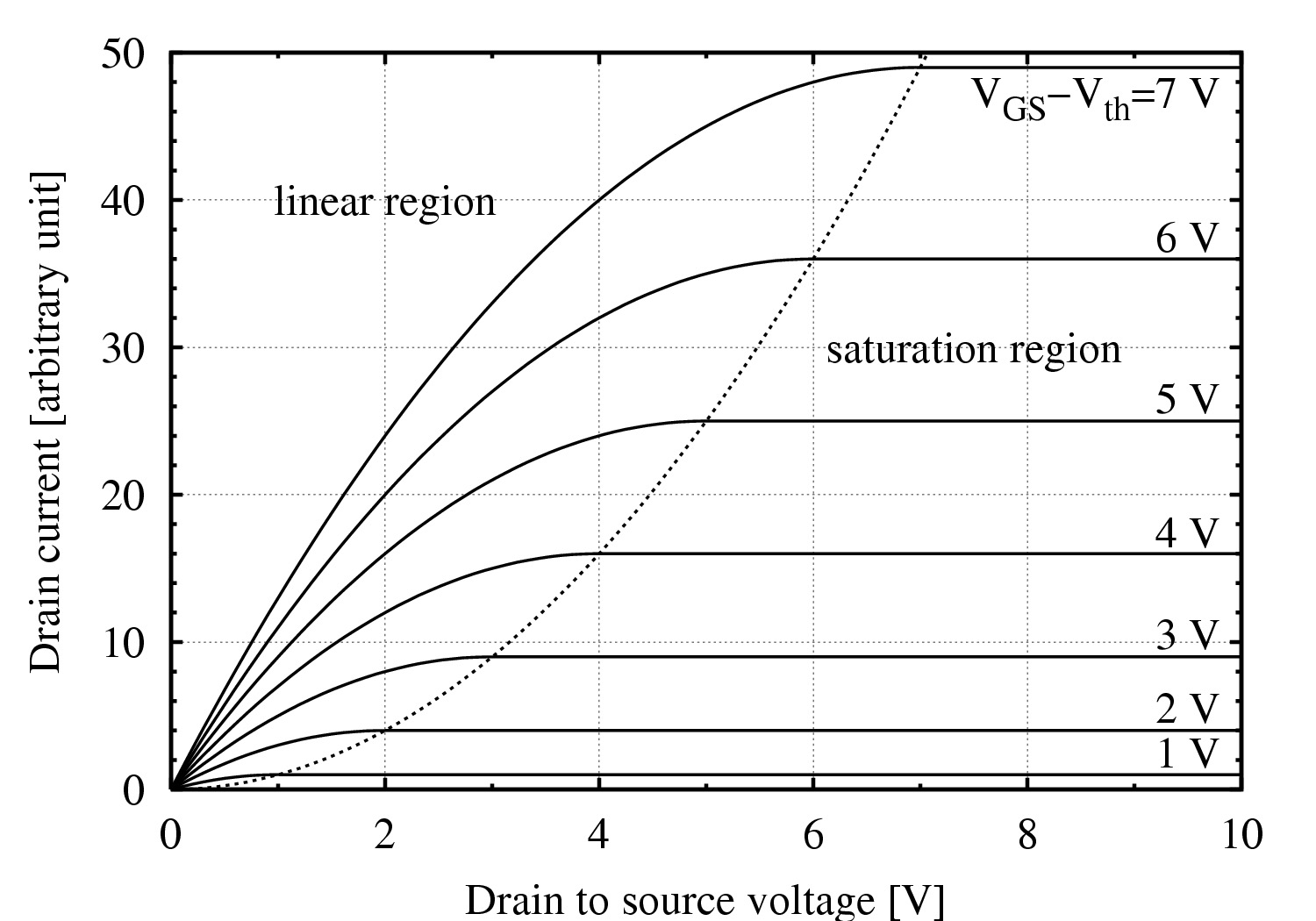
Ohmic or saturation: pick your region Ohmic , far left: a small resistance R D S ( o n ) \Rds R DS ( on )
Saturation , flat: current set by V G S V_{GS} V GS
Switches live in the ohmic region, amplifiers in saturation. Lab 4 is a switch.
© Ran Yang, Ph.D. Advanced Instrumentation
PHYS 351 · Lecture 04 33
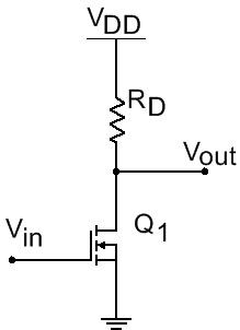
On or off, never in between P on = I D 2 R D S ( o n ) P off ≈ 0 P_{\text{on}} = I_D^{\,2}\,\Rds\qquad P_{\text{off}} \approx 0 P on = I D 2 R DS ( on ) P off ≈ 0 0.5 A through 0.54 Ω 0.54\ohm 0.54 Ω P = 0.135 P = 0.135 P = 0.135
A resistor halving the motor voltage at 0.5 A: 1.25 W of heat.
Halfway on is the one state that costs you.
© Ran Yang, Ph.D. Advanced Instrumentation
PHYS 351 · Lecture 04 34
The L in IRL510 The Pi can put only 3.3 V on the gate.
Many power MOSFETs want 10 V. At 3.3 V they half-conduct and get hot.
A logic-level part is fully on at 4–5 V. That is the L. The IRF510 is not.
Record from the datasheet
pins ⋅ \cdot ⋅ V GS(th) V_{\text{GS(th)}} V GS(th) ⋅ \cdot ⋅ R D S ( o n ) \Rds R DS ( on ) V G S V_{GS} V GS ⋅ \cdot ⋅ I D I_D I D ⋅ \cdot ⋅ V D S , max V_{DS,\max} V D S , m a x
© Ran Yang, Ph.D. Advanced Instrumentation
PHYS 351 · Lecture 04 35
4–5 V is not 3.3 V R D S ( o n ) \Rds R DS ( on )
Run the motor. Measure V D S V_{DS} V D S
Weak motor or a warm device means a gate driver or a level shift. Say what you found.
© Ran Yang, Ph.D. Advanced Instrumentation
PHYS 351 · Lecture 04 36
Low-side switching Supply → \rightarrow → → \rightarrow → Source to ground.
V G S V_{GS} V GS source . Source on ground: V G S V_{GS} V GS
MOSFET above the motor instead: the source rises as it turns on, V G S V_{GS} V GS
High side needs a gate driver. Not this lab.
© Ran Yang, Ph.D. Advanced Instrumentation
PHYS 351 · Lecture 04 37
Two small resistors that make it behave Gate series resistor , a few hundred ohms: limits the current pulse that charges the gate at every edge.
Pull-down , about 10 kΩ \Upomega Ω cleanup(), or if a wire falls out.
A floating gate drifts, and the motor switches itself on.
© Ran Yang, Ph.D. Advanced Instrumentation
PHYS 351 · Lecture 04 38
Two FETs make a logic gate
© Ran Yang, Ph.D. Advanced Instrumentation
PHYS 351 · Lecture 04 39
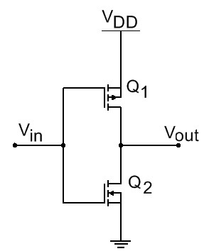
CMOS: a complementary pair p-channel above, n-channel below, gates tied together.
V i n V_{in} V in high .
V i n V_{in} V in low .
A NOT gate. Every gate is built this way.
© Ran Yang, Ph.D. Advanced Instrumentation
PHYS 351 · Lecture 04 40
Why the whole industry uses it In either steady state one of the two is off , so no current runs from
V D D V_{DD} V D D
P static ≈ 0 P dynamic ≈ C V 2 f P_{\text{static}} \approx 0 \qquad\qquad P_{\text{dynamic}} \approx C V^2 f P static ≈ 0 P dynamic ≈ C V 2 f That is why a processor’s power scales with clock speed, and why your laptop throttles.
© Ran Yang, Ph.D. Advanced Instrumentation
PHYS 351 · Lecture 04 41
You have been using one all along Lecture 03: “an output pin is a pair of transistors acting as a two-way switch.”
That pair is this CMOS inverter, on the Pi’s own die.
Push–pull is the same idea under another name.
Writing a 1 turns on the upper device; writing a 0 turns on the lower one.
The 16 mA limit is those two small transistors’ on-resistance and thermal rating, nothing more.
© Ran Yang, Ph.D. Advanced Instrumentation
PHYS 351 · Lecture 04 42
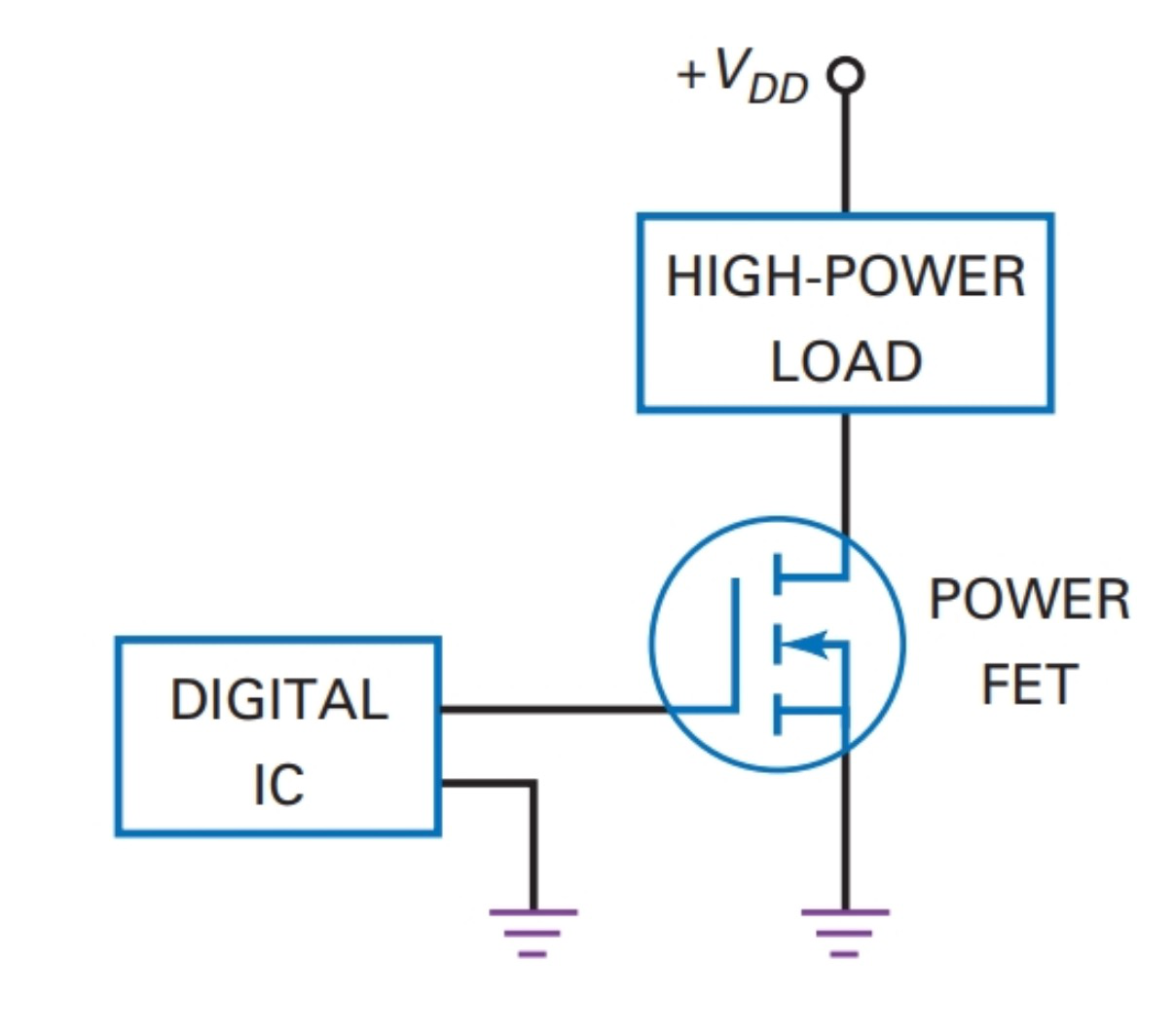
From logic to load The same device, scaled up: 1 A to 200 A, 1 W to 500 W.
A power FET is the standard interface between a logic output and a
motor, lamp, heater or solenoid.
Your Lab 4 circuit is this block diagram with real parts in it.
© Ran Yang, Ph.D. Advanced Instrumentation
PHYS 351 · Lecture 04 43
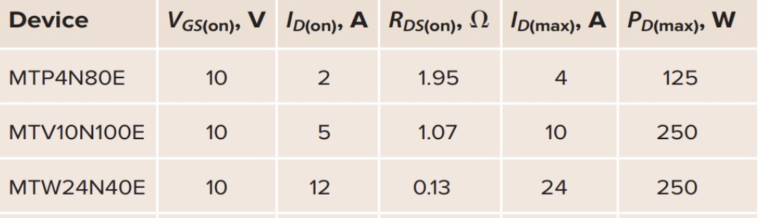
Reading a device table Notice what moves together: bigger current ratings come with smaller R D S ( o n ) \Rds R DS ( on ) V G S = 10 V_{GS} = 10 V GS = 10
© Ran Yang, Ph.D. Advanced Instrumentation
PHYS 351 · Lecture 04 44
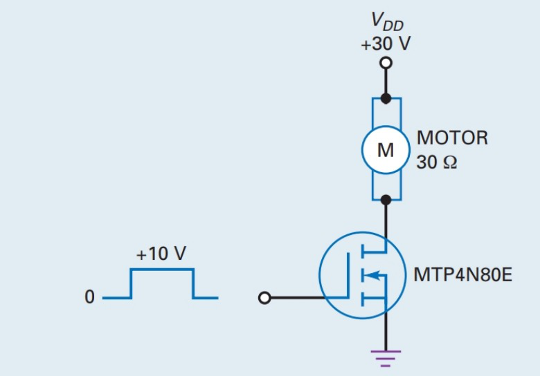
Worked example: what does the motor actually get? Ideal switch: 30 V / 30 Ω = 1.00 30\,\text{V} / 30\ohm = 1.00 30 V /30 Ω = 1.00
With R D S ( o n ) = 1.95 Ω \Rds = 1.95\ohm R DS ( on ) = 1.95 Ω
I D = 30 V 30 Ω + 1.95 Ω = 0.939 A I_D = \frac{30\,\text{V}}{30\ohm + 1.95\ohm} = 0.939\ \text{A} I D = 30 Ω + 1.95 Ω 30 V = 0.939 A Six per cent less, and 1.7 W in the transistor.
© Ran Yang, Ph.D. Advanced Instrumentation
PHYS 351 · Lecture 04 45
Check the region before you trust that That calculation assumes the device is ohmic , not saturated.
It holds only while the current the load allows is less than the current the gate
drive would permit: I D ( sat ) < I D ( on ) I_{D(\text{sat})} < I_{D(\text{on})} I D ( sat ) < I D ( on )
Confirm it from the datasheet, then use R D S ( o n ) \Rds R DS ( on )
© Ran Yang, Ph.D. Advanced Instrumentation
PHYS 351 · Lecture 04 46
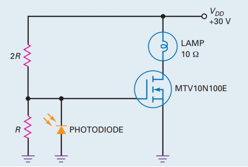
One more, and it is Lab 1 again Daylight: the photodiode conducts, the gate stays low, lamp off.
Night: the photodiode stops, the gate rises, lamp on.
A Lab 1 detector driving a Lab 4 switch.
© Ran Yang, Ph.D. Advanced Instrumentation
PHYS 351 · Lecture 04 47
Act 3 | Driving the motor
© Ran Yang, Ph.D. Advanced Instrumentation
PHYS 351 · Lecture 04 48
The component most often left out Switch off: the winding current has nowhere to go. V L = − L d I / d t V_L = -L\,\mathrm{d}I/\mathrm{d}t V L = − L d I / d t
The rule
Diode across the motor, reverse-biased by the supply : band to + + +
© Ran Yang, Ph.D. Advanced Instrumentation
PHYS 351 · Lecture 04 49
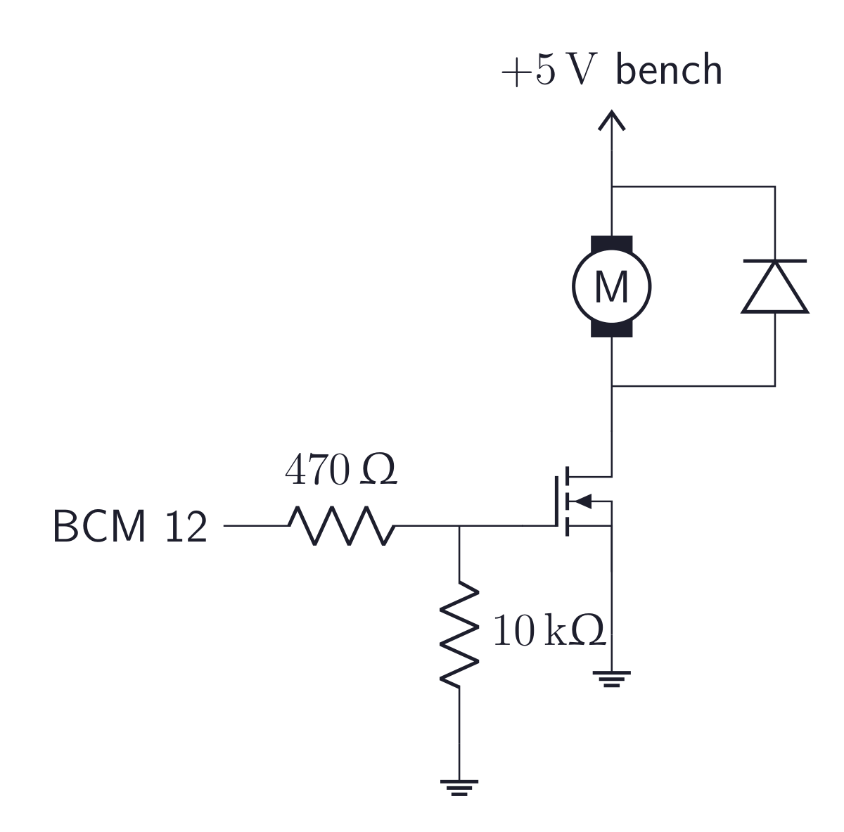
The complete circuit The motor runs from its own supply. The Pi sends only PWM.
Common ground is not optional
Pi GND and bench GND tied, or V G S V_{GS} V GS
© Ran Yang, Ph.D. Advanced Instrumentation
PHYS 351 · Lecture 04 50
Bring it up one thing at a time Task 2. Gate from a fixed + 5 +5 + 5
Instructor or TA checks the circuit before the motor is powered.
Task 3. Move the gate to BCM 12 through the gate resistor. Now only the signal path is under test.
© Ran Yang, Ph.D. Advanced Instrumentation
PHYS 351 · Lecture 04 51
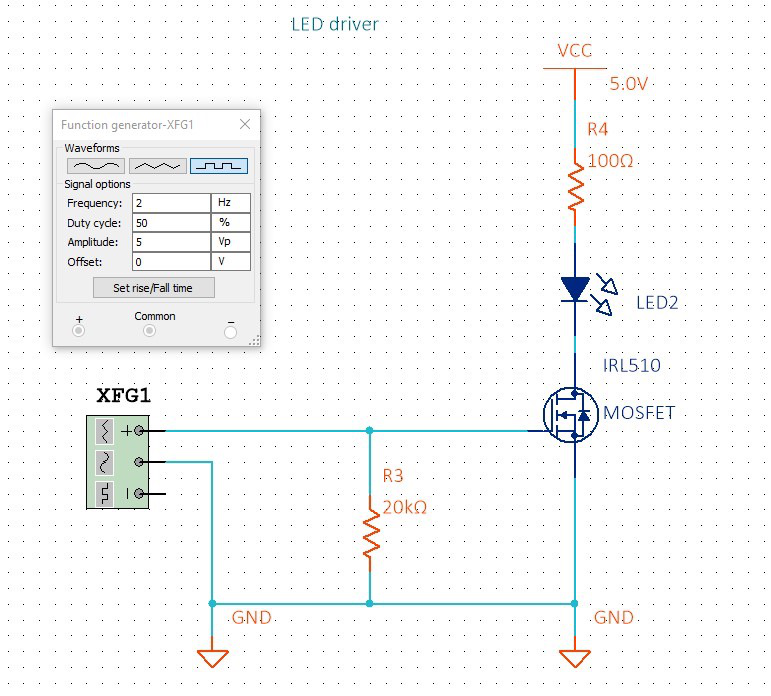
The same idea in Multisim Swap the LED for a motor, add the flyback diode, and this is Lab 4.
© Ran Yang, Ph.D. Advanced Instrumentation
PHYS 351 · Lecture 04 52
Measuring rotation
© Ran Yang, Ph.D. Advanced Instrumentation
PHYS 351 · Lecture 04 53
The Lab 1 detector becomes a tachometer LED on one side of the shaft, photodiode on the other, something that breaks the beam N N N
RPM = pulses N × t gate × 60 \text{RPM} = \frac{\text{pulses}}{N \times t_{\text{gate}}} \times 60 RPM = N × t gate pulses × 60 Or read the pulse period on the scope and invert it.
Wrong N N N
© Ran Yang, Ph.D. Advanced Instrumentation
PHYS 351 · Lecture 04 54
Make the pulses clean the TIA, not a bare resistor: gain, and a fixed diode bias shield from room light: fluorescents flicker at 120 Hz, right in your RPM range look on the scope before writing any counting code Two traps. Double counting on slow edges. Counting PWM edges instead of the shaft.
© Ran Yang, Ph.D. Advanced Instrumentation
PHYS 351 · Lecture 04 55
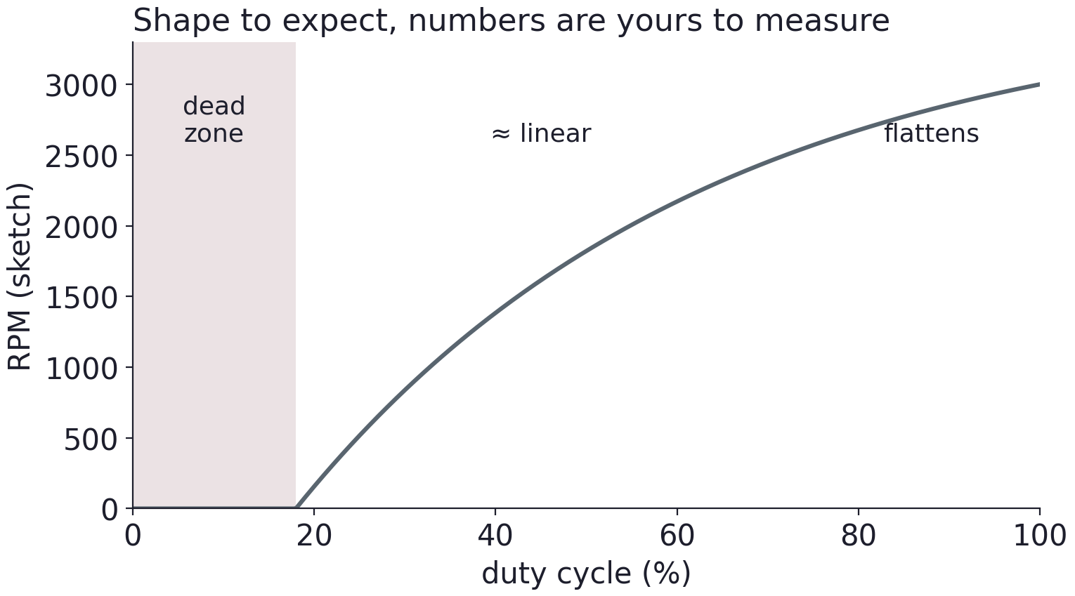
What the curve looks like RPM ≈ k ( D − D 0 ) \text{RPM} \approx k\,(D - D_0) RPM ≈ k ( D − D 0 ) Cluster points near the dead-zone edge.
Fit the linear region only; say which points.
k k k
© Ran Yang, Ph.D. Advanced Instrumentation
PHYS 351 · Lecture 04 56
Two extra results worth chasing Hysteresis. Sweep up from 0, then down from 100 %. The motor keeps turning below the duty that started it.
PWM frequency. The rotor’s time constant is tens of ms. Periods much shorter are averaged; comparable ones jerk. The reference code uses 50 Hz.
A null result honestly reported is still a result.
© Ran Yang, Ph.D. Advanced Instrumentation
PHYS 351 · Lecture 04 57
Measurement technique Measure How Watch out PWM gate signal probe BCM 12, DC coupling, statistics on AC coupling kills the duty reading Drain waveform probe the drain, clip on common ground spikes exceed the probe rating without the diode Motor current DMM in series on the supply side a time-average of a switched current Winding resistance DMM, motor disconnected varies with shaft position; quote a range Rotation rate pulse train on the scope confirm N N N
© Ran Yang, Ph.D. Advanced Instrumentation
PHYS 351 · Lecture 04 58
Destroys hardware Do not
leave out the flyback diode, or fit it backwards
Secure the motor. Eye protection on. Power off before touching anything mechanical.
© Ran Yang, Ph.D. Advanced Instrumentation
PHYS 351 · Lecture 04 59
Take away A BJT is a current valve and keeps charging you base current. A FET is a field valve: the gate is a capacitor, so holding it on is free.
Enhancement mode means normally off, and in the ohmic region a fully-on device is just a small resistance.
Give the load its own supply, tie the grounds, put a diode across anything inductive, and switch fully on or fully off.
© Ran Yang, Ph.D. Advanced Instrumentation
PHYS 351 · Lecture 04 60
Exit check 1. What does a MOSFET gate look like electrically, and why does that suit a 3.3 V pin?
2. Depletion or enhancement: which is normally on? Which do you want for a motor, and why?
3. Winding 2.5 Ω \Upomega Ω
4. In a CMOS inverter, why is the static power nearly zero?
© Ran Yang, Ph.D. Advanced Instrumentation
Use ← → to move, Home / End to jump, and F for fullscreen.
Figure descriptions Slide 14 · Rewind: doping makes carriers Phosphorus contributes five valence electrons to a silicon lattice. Four form bonds and the fifth becomes a free electron, creating N-type material.
Boron contributes three valence electrons to a silicon lattice, leaving an unfilled bond or hole, creating P-type material.
Slide 16 · The BJT: two junctions, three regions NPN transistor layers: an N-type collector and N-type emitter lie on either side of the thin P-type base.
Slide 17 · The BJT is controlled by current NPN bias circuit: VBB drives the base through RB, VCC supplies the collector through RC, and the emitter is grounded. Arrows identify base, collector, and emitter currents.
Slide 20 · The FET family FET family tree: JFETs operate in depletion mode and can be N- or P-channel. Insulated-gate MOSFETs include depletion and enhancement types; the N-channel enhancement branch identifies the IRL510.
Slide 22 · JFET: normally on, squeeze it shut JFET amplifier: drain resistor RD connects to the positive supply, source resistor RS connects to ground, and the signal enters the gate with bias resistor RG to ground.
Slide 23 · MOSFET: put glass under the gate N-channel MOSFET cross-section with no inversion channel: metal gate is separated from the p-type substrate by silicon dioxide; n-plus source and drain wells are disconnected through the surface.
Slide 24 · Enhancement: the field builds the channel N-channel MOSFET cross-section with positive gate bias: an inversion channel forms beneath the insulating oxide and connects the n-plus source and drain wells. An arrow identifies the channel.
Slide 26 · The same thing as a curve Conceptual FET transfer curves: an enhancement device is off near zero gate voltage and turns on above threshold; a depletion device conducts at zero gate voltage and can be turned off with negative bias.
Slide 28 · Why that comparison decides Lab 4 Conceptual comparison: BJT collector current rises with base current; FET drain current rises with gate-source voltage above threshold, with essentially no steady gate current.
Slide 31 · The symbol, and the diode you did not ask for N-channel power MOSFET symbol showing gate, drain, source, and the intrinsic body diode between source and drain.
Slide 32 · Ohmic or saturation: pick your region MOSFET output-characteristic family: drain current first rises with drain-source voltage in the linear region, then flattens in saturation. Larger gate-source voltages produce larger drain currents.
Slide 33 · On or off, never in between N-channel MOSFET inverter switch: a resistor pulls Vout up to VDD, the drain connects to Vout, the source is grounded, and Vin controls the gate.
Slide 39 · CMOS: a complementary pair CMOS inverter: an upper transistor connects the output to VDD and a lower transistor connects it to ground. Both gates share Vin and their joined drains form Vout.
Slide 42 · From logic to load Digital IC driving a grounded-source power FET. A high-power load connects between positive supply and drain, allowing a logic signal to switch load current.
Slide 43 · Reading a device table Comparison of three power MOSFETs, listing gate drive, drain current, on-resistance, maximum current, and power dissipation. The examples require 10 V gate drive and are not automatically suitable for direct 3.3 V GPIO control.
Slide 44 · Worked example: what does the motor actually get? Illustrative power-MOSFET motor driver: a motor connects between a 30 V supply and the drain, source is grounded, and a diode lies across the motor. The gate waveform is labeled 0 to 10 V.
Slide 46 · One more, and it is Lab 1 again Light-controlled lamp circuit: a photodiode and bias resistors set a MOSFET gate voltage; the MOSFET switches a lamp connected to a 30 V supply. This is an illustrative circuit, not Raspberry Pi wiring.
Slide 49 · The complete circuit Low-side motor driver: the motor lies between positive supply and MOSFET drain, source connects to ground, and the GPIO drives the gate through a resistor with a pull-down to ground. A flyback diode across the motor is reverse-biased during normal operation.
Slide 51 · The same idea in Multisim Simulated IRL510 low-side LED driver: a supply feeds a resistor and LED into the drain; the source is grounded, the gate receives a pulse waveform, and a gate pull-down holds it off when undriven.
Slide 55 · What the curve looks like Conceptual motor speed versus PWM duty: an initial dead zone is followed by an approximately linear rise and then flattening at high duty. Actual values must be measured.
Complete notes Lab 4 manual