PHYS 351 · Lecture 01-02 01
Lectures 01–02
From Photodiodes to Mixers Covers Labs 1 and 2
© Ran Yang, Ph.D. Advanced Instrumentation
PHYS 351 · Lecture 01-02 02
Today, in one line Sensor → \rightarrow →
Amplifier → \rightarrow →
Multiply + + + → \rightarrow →
© Ran Yang, Ph.D. Advanced Instrumentation
PHYS 351 · Lecture 01-02 03
Two ideas that run through the course Feedback turns a vague device into a predictable one.
Multiplication moves information in frequency.
Labs 1 and 2 are entirely analog. From Lab 3 a computer takes over the decisions.
© Ran Yang, Ph.D. Advanced Instrumentation
PHYS 351 · Lecture 01-02 04
Where each task points Task You build Idea Lab 1, 1.1 LED driver, 5.0 V max, current limited series resistor Lab 1, 1.2 the same driver with an op-amp feedback current control Lab 1, 2.1 photodiode + resistor; current at − 3.0 -3.0 − 3.0 photodiode model, sign Lab 1, 2.2 photodiode + op-amp transimpedance amplifier Lab 1, 3 analyse the given circuit: V a V_a V a V b V_b V b biased inverter + RC filter Lab 2, 1 AD633 product and squaring; quadratic fit multiplier equation Lab 2, 2 offset adjustment offset, scale, nonlinearity Lab 2, 3 squarer in a loop → \rightarrow → feedback inverts a function
© Ran Yang, Ph.D. Advanced Instrumentation
PHYS 351 · Lecture 01-02 05
Driving an LED
© Ran Yang, Ph.D. Advanced Instrumentation
PHYS 351 · Lecture 01-02 06
LED driver: limit the current An LED is not a safe load for a voltage source.
I LED = V source − V F R I_{\text{LED}} = \frac{V_{\text{source}} - V_F}{R} I LED = R V source − V F Design at the worst case : the top of the range.
© Ran Yang, Ph.D. Advanced Instrumentation
PHYS 351 · Lecture 01-02 07
Op-amp driver: feedback holds the current Sense the current across a resistor; the loop holds that voltage at a reference.
V F V_F V F
Check three limits
output inside the rails ⋅ \cdot ⋅ ⋅ \cdot ⋅
© Ran Yang, Ph.D. Advanced Instrumentation
PHYS 351 · Lecture 01-02 08
Detecting light
© Ran Yang, Ph.D. Advanced Instrumentation
PHYS 351 · Lecture 01-02 09
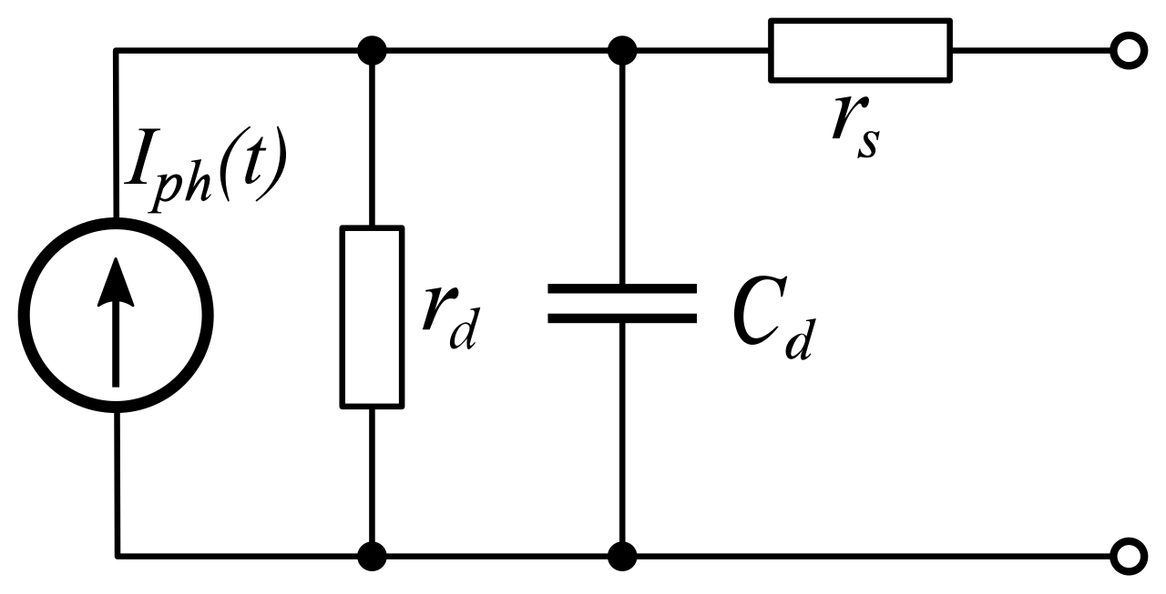
Photodiode: the model to keep A light-dependent current source in parallel with a diode.
More light, more current. Linear over many decades.
A resistor turns the current into a voltage.
© Ran Yang, Ph.D. Advanced Instrumentation
PHYS 351 · Lecture 01-02 10
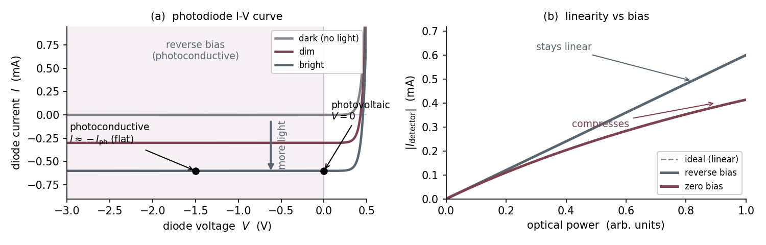
Why reverse bias helps Light shifts the whole curve down. On the flat part I ≈ − I ph I \approx -I_{\text{ph}} I ≈ − I ph
© Ran Yang, Ph.D. Advanced Instrumentation
PHYS 351 · Lecture 01-02 11
Resistor detector: the DMM reads − 3.0 -3.0 − 3.0 I = V det R det I = \frac{V_{\text{det}}}{R_{\text{det}}} I = R det V det Define the polarity and the current direction before the algebra.
A negative answer is a direction, not a mistake.
© Ran Yang, Ph.D. Advanced Instrumentation
PHYS 351 · Lecture 01-02 12
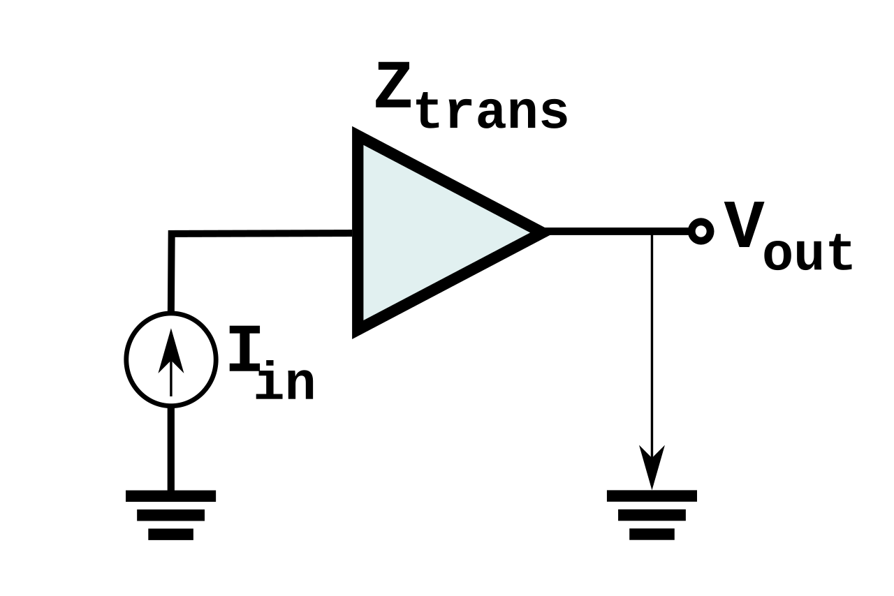
Photodiode + op-amp: the TIA V out = − I photo R f V_{\text{out}} = -\,I_{\text{photo}}\,R_f V out = − I photo R f Inverting input held at virtual ground.
The photocurrent has nowhere to go but R f R_f R f
The diode always sees the same bias.
© Ran Yang, Ph.D. Advanced Instrumentation
PHYS 351 · Lecture 01-02 13
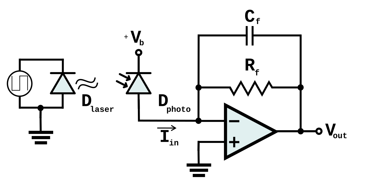
TIA: what limits it output swing inside the rails op-amp output current capacitance against R f R_f R f C f C_f C f Oscillating? This is why.
© Ran Yang, Ph.D. Advanced Instrumentation
PHYS 351 · Lecture 01-02 14
Lab 1 Task 3: two blocks in series 1. Biased inverting amplifier, referenced to V + V_+ V + not ground.
2. RC low-pass, f c = 1 / ( 2 π R 5 C 1 ) f_c = 1/(2\pi R_5 C_1) f c = 1/ ( 2 π R 5 C 1 )
∣ H ∣ = 1 1 + ( f / f c ) 2 φ = − arctan ( f / f c ) |H| = \frac{1}{\sqrt{1 + (f/f_c)^2}} \qquad \varphi = -\arctan(f/f_c) ∣ H ∣ = 1 + ( f / f c ) 2 1 φ = − arctan ( f / f c ) Show the lag in your sketch. Check nothing exceeds ± 15 \pm 15 ± 15
© Ran Yang, Ph.D. Advanced Instrumentation
PHYS 351 · Lecture 01-02 15
Multiplying signals
© Ran Yang, Ph.D. Advanced Instrumentation
PHYS 351 · Lecture 01-02 16
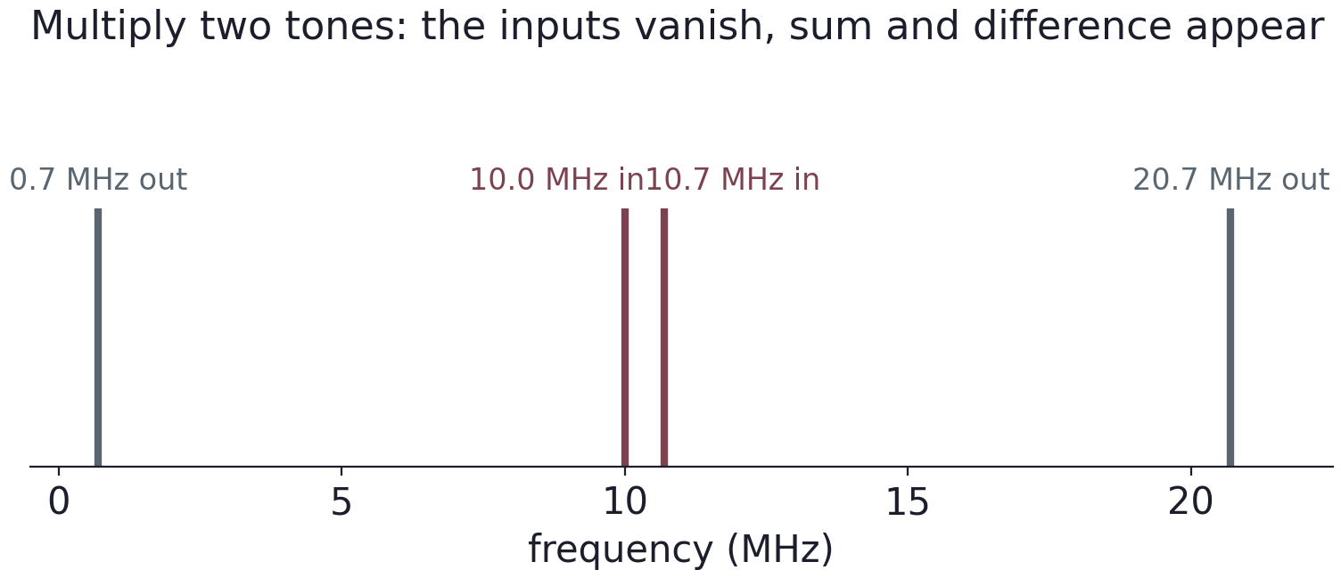
Multiply two tones cos ω 1 t cos ω 2 t = 1 4 ( e j ω 1 t + e − j ω 1 t ) ( e j ω 2 t + e − j ω 2 t ) = 1 2 [ cos ( ω 1 − ω 2 ) t + cos ( ω 1 + ω 2 ) t ] \begin{aligned}
\cos\omega_1 t\,\cos\omega_2 t
&= \tfrac14\Big(e^{j\omega_1 t}+e^{-j\omega_1 t}\Big)\Big(e^{j\omega_2 t}+e^{-j\omega_2 t}\Big)\\[2pt]
&= \tfrac12\big[\cos(\omega_1-\omega_2)t+\cos(\omega_1+\omega_2)t\big]
\end{aligned} cos ω 1 t cos ω 2 t = 4 1 ( e j ω 1 t + e − j ω 1 t ) ( e j ω 2 t + e − j ω 2 t ) = 2 1 [ cos ( ω 1 − ω 2 ) t + cos ( ω 1 + ω 2 ) t ] The inputs are gone. A difference tone and a sum tone remain.
© Ran Yang, Ph.D. Advanced Instrumentation
PHYS 351 · Lecture 01-02 18
Conversion loss Each output tone has amplitude A B / 2 AB/2 A B /2 A B AB A B
Half the amplitude, a quarter of the power: − 6 -6 − 6
The product’s power splits between two lines. Keep one, lose half.
So a mixer is followed by gain at the intermediate frequency.
© Ran Yang, Ph.D. Advanced Instrumentation
PHYS 351 · Lecture 01-02 19
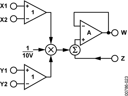
AD633 analog multiplier W = ( X 1 − X 2 ) ( Y 1 − Y 2 ) 10 V + Z W=\frac{(X_1-X_2)(Y_1-Y_2)}{10\ \text{V}}+Z W = 10 V ( X 1 − X 2 ) ( Y 1 − Y 2 ) + Z Differential inputs: ground the unused one.
÷ 10 \div 10 ÷ 10
0.1 μ 0.1\,\upmu 0.1 μ
© Ran Yang, Ph.D. Advanced Instrumentation
PHYS 351 · Lecture 01-02 20
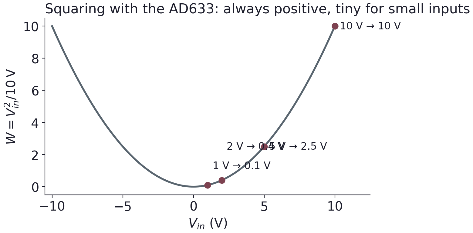
Tie the inputs together: a squarer W = V in 2 10 V W = \frac{V_{\text{in}}^2}{10\ \text{V}} W = 10 V V in 2 At V in = 1 V_{\text{in}} = 1 V in = 1
A 20 mV offset is then a 20 % error.
© Ran Yang, Ph.D. Advanced Instrumentation
PHYS 351 · Lecture 01-02 21
Fit the data, then read the coefficients W = a V in 2 + b V in + c W = a\,V_{\text{in}}^2 + b\,V_{\text{in}} + c W = a V in 2 + b V in + c a a a 1 / ( 10 V ) 1/(10\,\text{V}) 1/ ( 10 V )
b ≠ 0 b \neq 0 b = 0 ( V + ε ) 2 = V 2 + 2 ε V + ε 2 (V+\varepsilon)^2 = V^2 + 2\varepsilon V + \varepsilon^2 ( V + ε ) 2 = V 2 + 2 ε V + ε 2
c ≠ 0 c \neq 0 c = 0
© Ran Yang, Ph.D. Advanced Instrumentation
PHYS 351 · Lecture 01-02 22
Four error sources, four signatures Error Signature in the fit Fix Input offset linear term b b b trim at the unused input Output offset constant c c c opposing voltage at Z Z Z Scale factor a ≠ 0.100 V − 1 a \neq 0.100\,\text{V}^{-1} a = 0.100 V − 1 calibrate, or report it Nonlinearity a pattern in the residuals the device floor
Plot the residuals . On the raw data every fit looks perfect.
© Ran Yang, Ph.D. Advanced Instrumentation
PHYS 351 · Lecture 01-02 23
Square root by feedback Put a block that computes f ( ⋅ ) f(\cdot) f ( ⋅ )
The loop finds the output that makes the fed-back value match the input: it computes f − 1 ( ⋅ ) f^{-1}(\cdot) f − 1 ( ⋅ )
One polarity only. Worst accuracy near zero, where the slope of V 2 V^2 V 2
Task 3 wants offsets under ± 50 \pm 50 ± 50
© Ran Yang, Ph.D. Advanced Instrumentation
PHYS 351 · Lecture 01-02 24
Radio
© Ran Yang, Ph.D. Advanced Instrumentation
PHYS 351 · Lecture 01-02 25
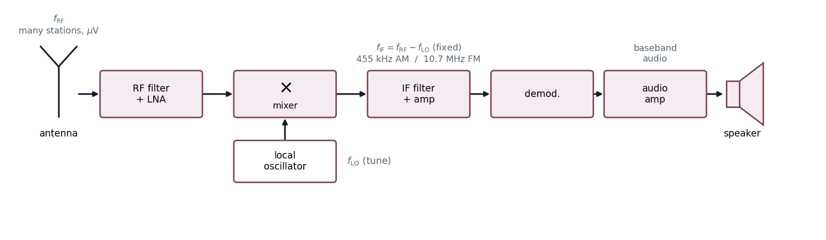
Inside a radio: the superhet chain Same front end for AM and FM; only the demodulator differs.
© Ran Yang, Ph.D. Advanced Instrumentation
PHYS 351 · Lecture 01-02 26
Tuning = set the LO ∣ f RF − f LO ∣ = f IF ( 455 kHz AM , 10.7 MHz FM ) |f_{\text{RF}} - f_{\text{LO}}| = f_{\text{IF}}\qquad
(455\,\text{kHz AM},\ 10.7\,\text{MHz FM}) ∣ f RF − f LO ∣ = f IF ( 455 kHz AM , 10.7 MHz FM ) All gain and selectivity live at one fixed IF.
The image at f LO ± f IF f_{\text{LO}} \pm f_{\text{IF}} f LO ± f IF
© Ran Yang, Ph.D. Advanced Instrumentation
PHYS 351 · Lecture 01-02 27
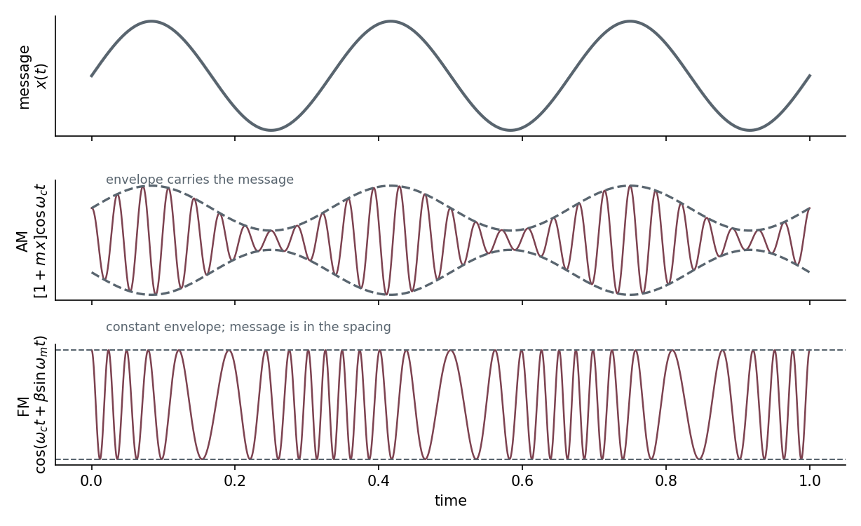
AM vs FM AM : message in the amplitude. Envelope detector.
FM : message in the frequency. Discriminator.
Constant envelope, so amplitude noise is ignored.
© Ran Yang, Ph.D. Advanced Instrumentation
PHYS 351 · Lecture 01-02 28
Take away Measure current across a known resistor.
Feedback turns a tiny current into a usable voltage, and inverts a function you cannot invert directly.
Multiply, then filter, to move a signal in frequency.
© Ran Yang, Ph.D. Advanced Instrumentation
PHYS 351 · Lecture 01-02 29
Exit check 1. − 2.0 -2.0 − 2.0 10 k Ω 10\kohm 10 k Ω
2. Why is V out = − I photo R f V_{\text{out}}=-I_{\text{photo}}R_f V out = − I photo R f
3. 5.0 5.0 5.0 4.3 4.3 4.3
4. Both AD633 inputs at − 3.0 -3.0 − 3.0 Z = 0 Z=0 Z = 0 W W W
© Ran Yang, Ph.D. Advanced Instrumentation
Use ← → to move, Home / End to jump, and F for fullscreen.
Figure descriptions Slide 9 · Photodiode: the model to keep Photodiode equivalent circuit: photocurrent source Iph is in parallel with diode resistance rd and capacitance Cd; series resistance rs connects that parallel network to the output terminal.
Slide 10 · Why reverse bias helps Photodiode current-voltage curves shift with illumination. A second plot compares output current versus optical power for ideal linear behavior, reverse bias, and zero bias.
Slide 12 · Photodiode + op-amp: the TIA Transimpedance amplifier block: input current Iin enters an amplifier with transimpedance Ztrans and produces output voltage Vout relative to ground.
Slide 13 · TIA: what limits it Photoconductive transimpedance circuit: a reverse-biased photodiode feeds the op-amp inverting input. Feedback resistor Rf and parallel capacitor Cf connect output to that input; the noninverting input is grounded.
Slide 17 · Try it: 10.7 MHz and 10.0 MHz Ideal mixing spectrum: inputs at 10.0 MHz and 10.7 MHz produce output components at the difference, 0.7 MHz, and sum, 20.7 MHz.
Slide 19 · AD633 analog multiplier AD633 multiplier: differential inputs X1 minus X2 and Y1 minus Y2 feed a multiplier scaled by 1/10 V. The Z input is added to produce output W.
Slide 20 · Tie the inputs together: a squarer AD633 squaring curve, W equals Vin squared divided by 10 V. Both input signs give nonnegative output; 1, 2, 5, and 10 V inputs give 0.1, 0.4, 2.5, and 10 V outputs.
Slide 25 · Inside a radio: the superhet chain Superheterodyne receiver chain: antenna, RF filter and amplifier, mixer fed by a local oscillator, intermediate-frequency filter and amplifier, demodulator, audio amplifier, and speaker.
Slide 27 · AM vs FM A slow message signal compared with amplitude and frequency modulation. In AM the carrier amplitude follows the message; in FM its amplitude stays constant while the spacing of cycles changes.
Complete notes Lab 1 manual Lab 2 manual