- Where These Two Labs Sit
- LED Driver Design
- The Photodiode Detector
- Photodiode Plus Op-Amp: the TIA
- Lab 1 Task 3: Circuit Analysis
- What a Multiplier Does
- The AD633 Analog Multiplier
- Squaring, and the Square Root by Feedback
- Error Sources and Offset Trimming
- From Multiplier to Mixer
- How a Radio Receiver Works
- Self-Check
- Practical Engineering Connections
1Where These Two Labs Sit
These first two labs are entirely analog. Everything that happens is decided by the hardware: a resistor sets a current, a feedback loop sets a gain, a multiplier forms a product. No software is involved anywhere, and that is deliberate — from Lab 3 onward a Raspberry Pi takes over the decision-making, and you will want a firm grip on what the analog front end is doing before you put a computer in front of it.
Two ideas run through both labs and recur for the rest of the course:
- Feedback turns a vague device into a predictable one. A bare LED has no well-defined operating current and a bare photodiode produces a current too small to read. Wrap either in a resistor or an op-amp loop and it becomes an instrument.
- Multiplication moves information in frequency. Multiplying two signals produces sum and difference tones. That single fact is the basis of every radio receiver ever built, and of the AD633 work in Lab 2.
A measurement chain is a sequence of deliberate conversions: light to current, current to voltage, voltage to a product, a product to a new frequency. At every step you choose a component value that makes the next step well behaved. Design from the quantity you want to end up with, and work backwards.
1.1 Task map
| Task | What you build | Concept & section |
|---|---|---|
| Lab 1.1 | Adjustable LED driver, 5.0 V maximum, current limited | Series current limiting (§2.1) |
| Lab 1.2 | The same driver built around an op-amp | Feedback current control (§2.2) |
| Lab 2.1 | Photodiode and resistor light detector; find the current for a −3.0 V reading | Photodiode model, reverse bias, sign conventions (§3) |
| Lab 2.2 | Photodiode with an op-amp | Transimpedance amplifier (§4) |
| Lab 3 | Analyse the given op-amp circuit; find Va and Vb; sketch and simulate | Biased inverting stage plus RC low-pass (§5) |
| Lab 2, Task 1 | AD633 product and squaring function; quadratic fit | Multiplier transfer equation (§6–8) |
| Lab 2, Task 2 | Offset-adjustment circuit | Offset, scale-factor and linearity errors (§9) |
| Lab 2, Task 3 | Squarer inside a feedback loop to make a square root | Inverting a function with feedback (§8.3) |
2LED Driver Design
An adjustable LED driver has to hold the current to a safe value across its whole adjustment range. An LED is not a safe load for a voltage source: near its forward voltage, a small change in voltage produces a large change in current, because the diode characteristic is exponential.
2.1 The series-limited circuit
For a simple series-limited circuit the current follows from Kirchhoff's voltage law:
Design from the current limit first, at the worst case — the top of your adjustment range, where the source voltage is highest and the current therefore largest:
Lab 1 asks you to limit the voltage applied to the LED to 5.0 V and to include current limiting. Those are two separate requirements and they need two separate pieces of reasoning — one about the maximum node voltage your adjustment can produce, one about the maximum current at that setting. A design that satisfies only one of them will not pass.
2.2 Op-amp current control
In an op-amp version, negative feedback drives the output until a sensed voltage matches a reference. If the sensed voltage is the drop across a resistor carrying the LED current, then fixing that voltage fixes the current — and it stays fixed regardless of the LED's forward voltage, its temperature, or the exact supply.
That is the whole advantage over Equation (1): the series resistor sets a current that depends on VF, and VF drifts. The feedback loop sets a current that depends on a resistor and a reference, both of which are stable.
Three constraints bound the design and must all be checked:
- The op-amp output must stay within its supply rails.
- The LED current must stay within the LED's rating.
- The current must stay within the op amp's own output-current limit — a common oversight, since many general-purpose op amps will not deliver more than 20–25 mA.
(a) A supply adjusts from 0 to 9 V and the LED has VF = 2.0 V. Choose a series resistor so the current never exceeds 20 mA, and state the current at the top of the range.
(b) For that same resistor, what is the current when the supply is set to 4 V? Comment on how linearly the brightness tracks the adjustment knob.
(c) Explain in two sentences why the op-amp version holds the current steadier than the series resistor when the LED warms up and VF falls by 0.1 V.
3The Photodiode Detector
3.1 The physical model
Use this model and almost everything follows:
photodiode = a light-dependent current source, plus non-ideal diode behaviour
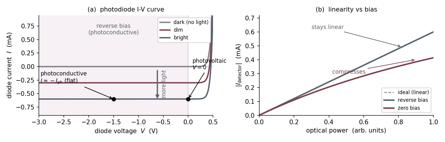
More light means more photocurrent, and the relationship is remarkably linear over many decades. Reverse biasing the diode lowers its junction capacitance and keeps the response linear, so the photocurrent is easier to interpret. A series resistor converts that current into a voltage a DMM or oscilloscope can read.
3.2 The I–V curve and why reverse bias helps
The photodiode current is the ordinary diode characteristic with the photocurrent subtracted:
Light shifts the whole curve down by Iph, so the device operates in the fourth quadrant — positive voltage, negative current, meaning it delivers power rather than absorbing it. That is the same effect that makes a solar cell work.
| Operating mode | Bias | Behaviour |
|---|---|---|
| Photovoltaic | zero bias | No bias-driven dark current, so the noise is low. But the junction capacitance is large and the detector is slow, and near the knee the response compresses at high light levels. |
| Photoconductive | reverse bias | The wider depletion region lowers junction capacitance and raises bandwidth; the response stays linear in optical power; and the diode cannot forward-bias as the output swings. The cost is dark current. |
Dark current is leakage that flows with no light at all, from thermally generated carriers and surface leakage. It grows with reverse voltage and roughly doubles every 10 °C. In a transimpedance amplifier it appears as an output offset of −IdarkRf plus shot noise of √(2qIdarkB), and together those set the smallest signal you can detect.
3.3 The DMM calculation, and what the sign means
Lab 1 Task 2 asks for the current when the DMM reads −3.0 V. Define the voltage polarity and the current reference direction before doing any algebra. With the reference direction taken through the detector resistor,
A negative value does not mean you made an arithmetic mistake, and it does not mean the current is somehow imaginary. It means the true polarity, and therefore the current direction under your stated convention, is opposite to the one you assumed. The current still has a definite magnitude and a definite physical direction.
Write the convention down in your report, in words or on the schematic, then quote the signed result and say what it implies physically. “I = −0.30 mA, i.e. 0.30 mA flowing from ground into the node” is a complete answer; “0.30 mA” alone is not.
A detector resistor reads −3.0 V. In terms of Rdet, Equation (4) gives Iphoto = −3.0 V / Rdet. For Rdet = 10 kΩ:
300 µA is a large photocurrent — this is a brightly illuminated detector, not a dim one. Sanity-check the magnitude against what you would expect: typical indoor light on a small photodiode gives microamps, not hundreds of microamps.
(a) Repeat the worked example for Rdet = 100 kΩ. Why might a larger resistor be chosen, and what does it cost you?
(b) The detector resistor is increased until the voltage across it approaches the reverse-bias supply. What happens to the linearity of the detector, and why?
(c) A datasheet quotes a dark current of 2 nA at 25 °C. Estimate it at 45 °C and state the offset it would produce across a 100 kΩ detector resistor.
4Photodiode Plus Op-Amp: the TIA
A transimpedance amplifier turns detector current straight into a measurable voltage. The photodiode connects to the inverting input, a feedback resistor Rf runs from the output back to that same input, and the non-inverting input is grounded.
With negative feedback the inverting input is held at virtual ground. The op-amp input current is approximately zero, so all of the photocurrent must flow through the feedback resistor, giving
More light gives a larger output, up to the point where the op amp runs out of voltage swing or output current.
4.1 Practical limits
- Output swing. The op amp cannot drive its output past the supply rails, so IphotoRf must stay inside them. This is what caps your usable gain.
- Output current. The op amp must supply the feedback network and any attached load without overload.
- Bandwidth and capacitance. The diode capacitance and the op amp's input capacitance work against Rf to cut bandwidth, and can make the amplifier ring or oscillate outright. A small capacitor across Rf restores the phase margin. If your TIA oscillates on the breadboard, this — not a wiring fault — is usually the reason.
The resistor detector is simple and entirely passive, but the voltage it develops changes the voltage across the diode, which disturbs the very thing being measured, and its gain and bandwidth are coupled.
The TIA sets the gain with one resistor and holds the photodiode node at a fixed voltage, so the diode always sees the same bias no matter how bright the light. That decoupling is the real reason the op-amp version is better, and it is worth a sentence in your discussion.
5Lab 1 Task 3: Circuit Analysis
Task 3 gives you an op-amp circuit and asks for Va and Vb, a sketch of Vin, Va and Vb over at least two periods, an explanation of each functional block, and a Multisim comparison. The supply rails are ±15 V and Vin is a 10 kHz sine wave of 1 V peak amplitude, with
The circuit is two functional blocks in series: a biased inverting amplifier followed by an RC low-pass filter. Identifying those two blocks is most of the work; naming them is explicitly part of what the task asks for.
5.1 The steps to follow
- Determine the non-inverting reference voltage V+ from the resistor divider. This sets the DC level that the amplified signal rides on.
- Derive Va using the inverting-amplifier relation referenced to V+, not to ground. This is the step most people get wrong.
- Find the cutoff frequency of the R5C1 low-pass network, fc = 1/(2πR5C1).
- Determine the magnitude and phase of the low-pass response at 10 kHz. Both matter — the phase shift is visible in your sketch.
- Use the response to write the filtered output Vb(t), as an explicit function of time.
- Check that the predicted signals stay within the ±15 V supply rails. If they do not, the real circuit clips and your sketch must show that.
For a single-pole low-pass filter at frequency f, with fc = 1/(2πRC):
A negative phase means the output lags the input. Show that lag in your sketch — two curves drawn exactly in phase is a giveaway that the phase was never computed.
Carry symbols as far as you can before substituting numbers, so the structure of the answer stays visible. Quote Va and Vb as explicit time functions with amplitude, DC offset and phase. Draw all three traces on one set of axes with a labelled voltage scale, so the gain and the offset can be read off. Then overlay the Multisim result and comment on any difference — a small discrepancy traced to a real cause is worth more than a perfect match asserted without checking.
6What a Multiplier Does
Lab 2 is built on one piece of trigonometry. Start with two tones:
Write each cosine with Euler's formula, cos θ = ½(ejθ + e−jθ), multiply out, and the four exponential terms pair back up into two real cosines:
A difference tone at f1 − f2 and a sum tone at f1 + f2. The original input frequencies are gone.
The raw product xy swings up to AB, but each output tone has amplitude only AB/2 — the amplitude is halved. Because power goes as amplitude squared, each tone carries (½)² = ¼ of the AB-amplitude power, which is 6 dB down. Equivalently: the product's power splits equally between the sum and difference lines, so keeping only one of them throws away half of it.
That split is the origin of a mixer's conversion loss, and it is why a mixer is normally followed by gain at the intermediate frequency.
(a) Determine the two output frequencies when f1 = 10.7 MHz and f2 = 10.0 MHz. Which circuit element selects the one you want?
(b) Both inputs are 2 V amplitude. What is the amplitude of each output tone before any scaling, and how many dB is that below AB?
(c) Set f1 = f2 in Equation (7). What are the two output terms, and what does the first one physically represent? (This is the squaring case — §8.)
7The AD633 Analog Multiplier
The AD633 is a four-quadrant analog multiplier — “four-quadrant” meaning both inputs may be either polarity and the output sign comes out right in all four combinations. Its transfer equation is
Two features of Equation (8) matter for every measurement in Lab 2. The inputs are differential — it is the difference X1 − X2 that is multiplied, so the unused input of a pair must be tied to a defined potential, normally ground, and not left floating. And the 10 V denominator scales the product down by ten before the Z input is added, which keeps the output inside the supply rails for inputs up to ±10 V.
| Pin | Function | Pin | Function |
|---|---|---|---|
| 1 | X1 — non-inverting X input | 8 | +VS — positive supply |
| 2 | X2 — inverting X input | 7 | W — product output |
| 3 | Y1 — non-inverting Y input | 6 | Z — summing input |
| 4 | Y2 — inverting Y input | 5 | −VS — negative supply |
This map is for the 8-lead PDIP package; the SOIC package uses a different arrangement. Check the package marking against the datasheet before wiring — swapping a supply pin for a signal pin destroys the part.
Lab 2 Task 1 explicitly asks for roughly 0.1 µF on each supply rail. Place each capacitor physically close to its supply pin — within a centimetre or so, not across the breadboard. Long leads have inductance, which defeats the purpose. Without decoupling, an analog multiplier is prone to oscillation that shows up as a fuzzy output trace and ruins the accuracy measurements you are about to take.
8Squaring, and the Square Root by Feedback
8.1 Tying the inputs together
Connect the two inputs together so that X1 − X2 = Y1 − Y2 = Vin, and set Z = 0. Equation (8) becomes
The output is always positive, whichever sign the input has — a good first test that the part is wired correctly and that your offsets are small.
Predict a few points from Equation (9) before you measure, so you know what “working” looks like:
| Vin | ±1 V | ±2 V | ±5 V | ±10 V |
|---|---|---|---|---|
| W | 0.10 V | 0.40 V | 2.50 V | 10.0 V |
Note how small the output is for small inputs: at Vin = 1 V it is only 100 mV. A 20 mV offset is then a 20% error. This is why the offset work in Task 2 matters, and why Task 3 insists offsets be under ±50 mV before you attempt the square root.
8.2 Fitting the data
Task 1 asks for a quadratic curve fit with your Python code and plot. Fit the general form rather than forcing it through the origin:
Each coefficient then means something physical, and that interpretation is the real content of the task: a should be 1/(10 V) — any departure is scale-factor error; a non-zero b reveals an input offset, since (V + ε)² expands to V² + 2εV + ε²; and a non-zero c is an output offset. Report all three with units and say what each one tells you about the device.
8.3 The square root by feedback
Task 3 asks you to put the squaring circuit inside a feedback loop to produce the inverse function. The principle is general and worth stating plainly:
Place a block that computes f(·) in the feedback path of a high-gain amplifier, and the closed loop computes f−1(·). The loop drives its output to whatever value makes the fed-back quantity match the input — so if the feedback block squares, the loop must be delivering a square root.
This is the same trick that makes a log amplifier from a diode's exponential characteristic. You are not designing a square-root circuit; you are letting feedback solve the equation W(Vout) = Vin for you.
Two practical consequences follow directly. The loop only works over the range where the squarer is monotonic, which means one polarity only — the square root of a negative number has no place to go, and the circuit will latch if you ask for it. And because the derivative of V² vanishes at the origin, loop gain collapses near zero input, so accuracy is worst there. Expect your square-root fit to be poorest at the low end, and say so.
9Error Sources and Offset Trimming
Lab 2 Task 2 names three error sources. Keep them distinct — they have different signatures in your data and different fixes.
| Error | What it is | Signature in a squaring measurement | Fix |
|---|---|---|---|
| Input offset | A small unwanted voltage added at an X or Y input | A linear term b in the quadratic fit; the output minimum sits away from Vin = 0 | Trim network injecting a small opposing voltage at the unused input of the pair |
| Output offset | A fixed voltage added to W | A non-zero constant c; output does not reach zero for zero input | Inject an opposing voltage at the Z pin |
| Scale-factor error | The divisor is not exactly 10 V | a differs from 0.100 V−1; error grows in proportion to the output | Calibrate — or simply report the measured scale factor |
| Nonlinearity | Residual departure from a true product, after the above are removed | Structure left in the fit residuals — not scatter, but a pattern | Cannot be trimmed out; it is the device's floor |
Plot the residuals — measured minus fitted — not just the data and the fit curve. On a plot of the raw data a good fit and a mediocre one look identical, because the quadratic dominates everything. On a residual plot, offset shows as a tilt or a shift, and nonlinearity shows as a smooth systematic curve that random noise cannot explain. One residual plot will tell your reader more than three pages of description.
Then report your offsets numerically and confirm they are within the ±50 mV that Task 3 requires before you proceed.
(a) A quadratic fit returns a = 0.0965 V−1, b = 0.018, c = −0.032 V. State the scale-factor error as a percentage, and estimate the input offset ε from b.
(b) With those coefficients, what output would you measure at Vin = 0? At Vin = 1 V, what is the percentage error relative to the ideal Equation (9)?
(c) Explain why the same absolute offset matters far more at Vin = 1 V than at Vin = 10 V.
10From Multiplier to Mixer
A mixer is a multiplier used deliberately to move a signal in frequency. The AD633 makes the multiplication explicit and visible, which is why Lab 2 uses it; a purpose-built radio mixer does the same job with a nonlinear switching core.
Both the sum and the difference appear at the output, and a filter keeps whichever one is wanted. Crucially, any modulation on the original signal rides along to the new frequency — the shift carries the information with it, which is the entire point.
10.1 The NE602/SA602 integrated mixer
This family packages the same idea into one IC. Its blocks are worth knowing because they reappear in every receiver front end:
- Local oscillator — an internal oscillator, or an external signal, provides the mixing frequency.
- Differential signal ports — the RF and oscillator inputs are differential, so coupling, biasing and the termination of unused inputs all matter.
- Nonlinear mixer core — an internal switching or transconductance structure creates the sum and difference products.
- Output network — external tuned circuits select the wanted intermediate frequency and reject the rest.
- Supply decoupling — a bypass capacitor close to the supply pins keeps supply noise and oscillator currents out of the signal path.
The mixer core does not produce only the frequency you want. A working design still needs a frequency plan, output filtering, sensible signal levels, correct biasing, and decoupling.
11How a Radio Receiver Works
Almost every radio is a superheterodyne receiver: it moves every station down to one fixed intermediate frequency before doing the selectivity and the gain. This is the payoff for everything in §6–10.
The mixing itself is neither AM nor FM. The RF filter, local oscillator, mixer and IF chain are identical for both — the mixer only translates the spectrum and carries whatever modulation is present along with it. AM and FM part ways only at the demodulator: AM is followed with an envelope detector, FM with a frequency discriminator, whose constant envelope makes FM immune to amplitude noise.
11.1 Choosing the local oscillator
The receiver keeps the difference frequency, and it must equal the IF:
For a wanted station there are therefore two solutions, because the oscillator may sit above or below it: fLO = fRF + fIF (high-side injection) or fLO = fRF − fIF (low-side). Both place the station on the IF. Broadcast AM receivers use high-side injection so the oscillator tunes over a smaller frequency ratio across the band. Since fIF is fixed, retuning the radio means changing fLO — nothing else moves. Broadcast AM uses 455 kHz; broadcast FM uses 10.7 MHz.
11.2 The image frequency
The mixer only sees |fRF − fLO|, so it cannot distinguish a signal above the oscillator from one the same distance below it. A second input — the image — also lands on the IF:
The image always sits 2fIF away from the wanted station, and rejecting it is the job of the RF pre-selector. A higher IF moves the image further away and makes that filtering easier — one reason broadcast FM uses 10.7 MHz.
- High-side: fLO = 1000 + 455 = 1455 kHz. The wanted station is at fLO − fIF = 1000 kHz and the image at fLO + fIF = 1910 kHz, since |1910 − 1455| = 455.
- Low-side: fLO = 1000 − 455 = 545 kHz. The station is at fLO + fIF = 1000 kHz and the image at fLO − fIF = 90 kHz, since |90 − 545| = 455.
In both cases the image sits 2fIF = 910 kHz from the wanted station.
(a) A receiver has fIF = 455 kHz and is tuned to a station at 1200 kHz using high-side injection. Find fLO and the image frequency, and state how far the image lies from the wanted station.
(b) Repeat for an FM receiver with fIF = 10.7 MHz tuned to 99.3 MHz. Is the image inside or outside the commercial FM band, and why does that matter for the pre-selector?
(c) A designer proposes lowering the IF to 100 kHz to get sharper IF filtering. What does this cost, quantitatively, in image rejection?
12Self-Check
- Why is an LED an unsafe load for a voltage source, and what does a series resistor change about that?
- State the two separate requirements in Lab 1 Task 1.1 and the calculation each one demands.
- A detector resistor reads −2.0 V across 10 kΩ. What is the current under the stated reference direction, and what does the sign mean physically?
- Give two concrete advantages of reverse-biasing a photodiode, and the price you pay.
- Why does a transimpedance amplifier produce Vout = −IphotoRf? Where does the minus sign come from, and what holds the input at virtual ground?
- Name the two functional blocks in the Lab 1 Task 3 circuit and state what each contributes to Vb.
- What frequencies result when 5.0 MHz and 4.3 MHz are multiplied, and which circuit element selects one of them?
- For the AD633 with Z = 0 and both inputs tied to 3.0 V, what is W? What if both are tied to −3.0 V?
- In a quadratic fit to squaring data, what does a non-zero linear coefficient tell you, and how would you correct it in hardware?
- A receiver has fIF = 455 kHz and fLO = 1355 kHz. Which station is being received, and where is the image?
Measure current through a known resistance; use feedback to convert small currents into useful voltages and to invert a function you cannot invert directly; and use multiplication plus filtering to translate a signal to a new frequency. Every one of those is a deliberate conversion with a component value chosen to make the next stage well behaved.
13Practical Engineering Connections
- LED drivers. Current limiting appears in status indicators, infrared remote controls, barcode scanners, optical encoders and fibre-optic transmitters. The driver protects the LED and makes its optical output predictable.
- Photodiode detectors. A photodiode and resistor form the front end of light meters, smoke detectors, automatic brightness controls, optical interrupters and IR receivers.
- Transimpedance amplifiers. TIAs appear in fibre-optic receivers, laser-power monitors, pulse oximeters, imaging sensors and high-speed optical links — anywhere a small detector current must become a low-noise voltage.
- Biased amplifier plus RC filter. The Lab 1 Task 3 chain is a basic sensor-conditioning circuit: remove offsets, set the signal range, limit bandwidth, prepare a sensor signal for an ADC. You will build the digital half of exactly this in Lab 8.
- Analog multipliers. The AD633 supports amplitude modulation, synchronous detection, phase-sensitive measurement, voltage-controlled gain, analog computation, and true-RMS or power measurement.
- Function inversion by feedback. The square-root loop is the same principle behind log and antilog amplifiers, automatic gain control, and analog linearisation of nonlinear sensors.
- Frequency mixers. Radio receivers and transmitters, software-defined radios, radar, and test instruments all mix signals to move information to a frequency that is easier to filter and amplify.
- System-level design. A real product combines current limiting, biasing, feedback, filtering, supply decoupling, calibration and protection. Getting the equation right is only part of the job — which is the theme of the whole course.
PHYS 351 · Lectures 01–02 Notes · © Ran Yang, Ph.D. · yangran.org/teaching/phys351/