Part 1 · Lab 1: set a current, then read one
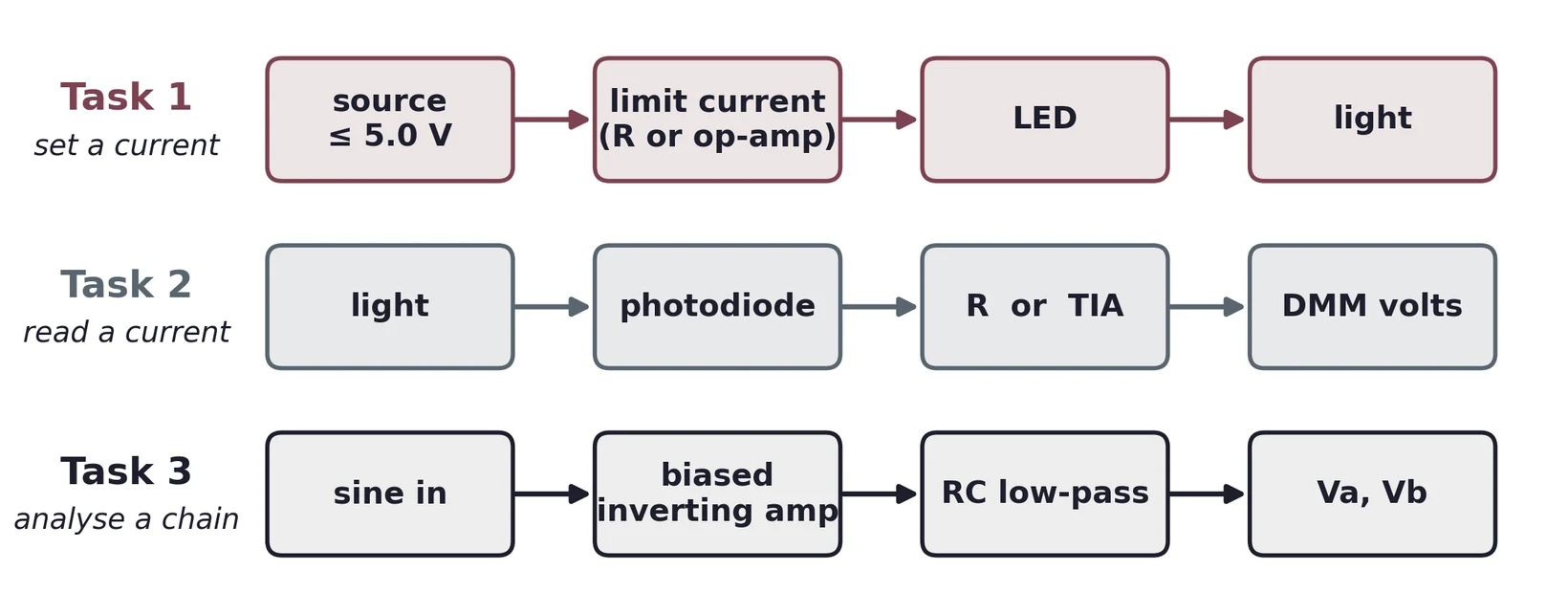
An LED needs a controlled current in. A photodiode gives a small current out. Both jobs are current handling, done first with a resistor, then with an op-amp.
An LED is a diode that emits light
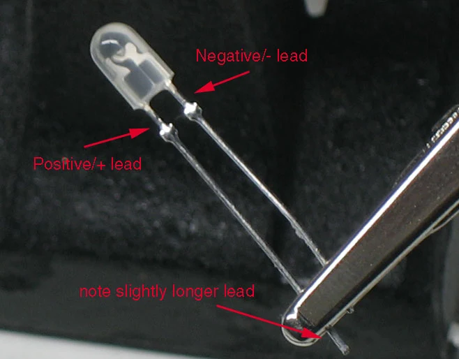
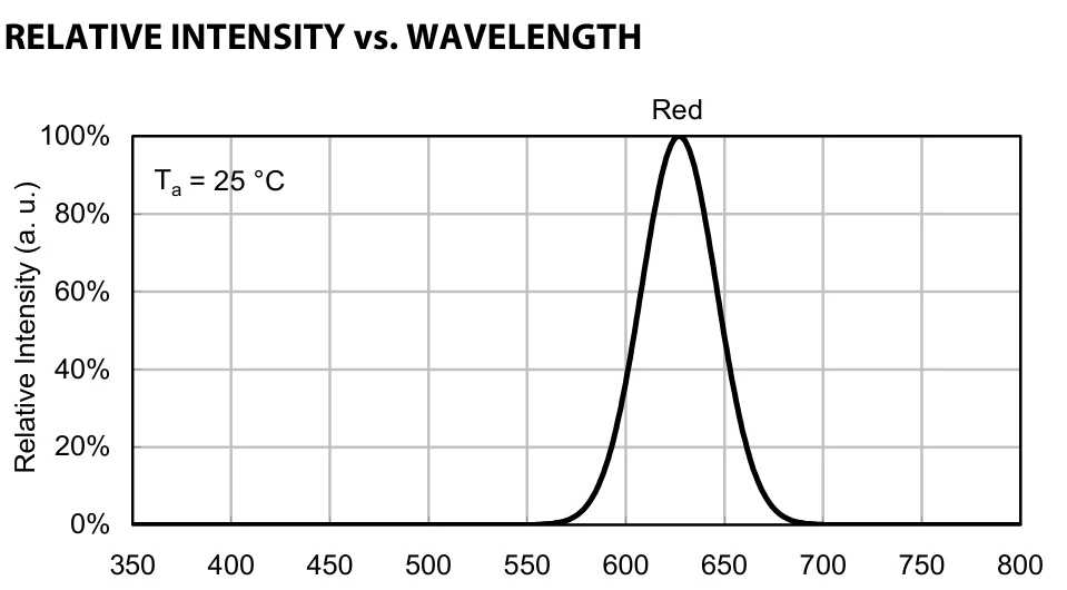
Electrons meet holes and give up the gap energy as light.
Current rises exponentially with voltage
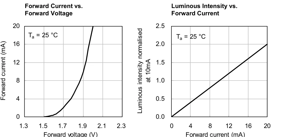
1.7 V gives about 4 mA; 2.0 V about 20 mA. Light follows current, so set the current. = 1.9 V typ, 2.3 V max at 10 mA.
Read the limits before you design
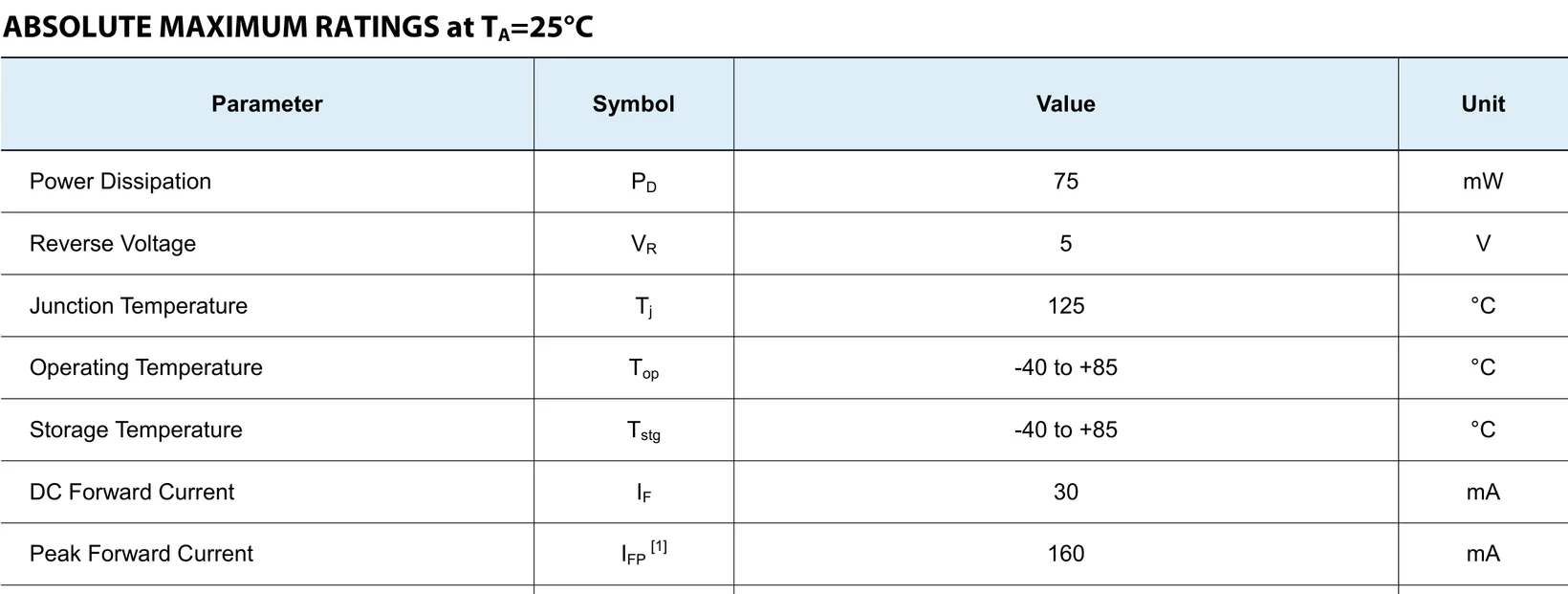
30 mA DC and 75 mW at most, and only 5 V in reverse: never put an LED backwards across a supply. Your LED may differ: measure it.
A series resistor turns a voltage into a current
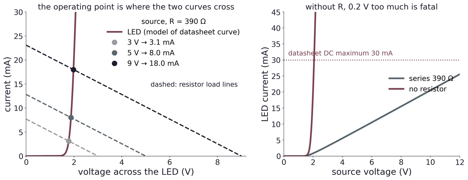
The load line crosses the LED curve at one point. With , current grows steadily with ; without it, a fraction of a volt too much burns the LED.
Adjustable but capped: a divider sets the top voltage
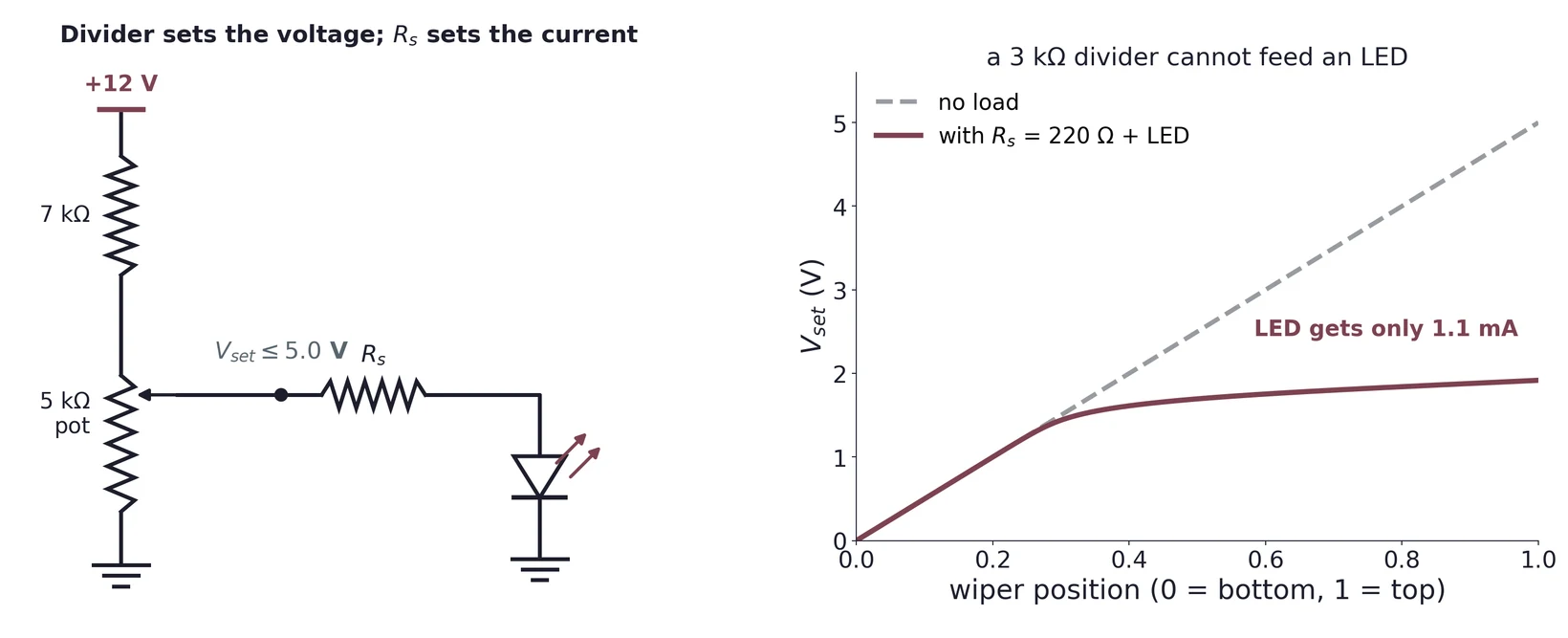
Unloaded, V at the top. But the divider's own 2.9 kΩ source resistance sits in series with the LED, so the node sags to about 2 V and the LED gets 1.1 mA.
Part 2 · The op-amp: huge gain, almost no input current
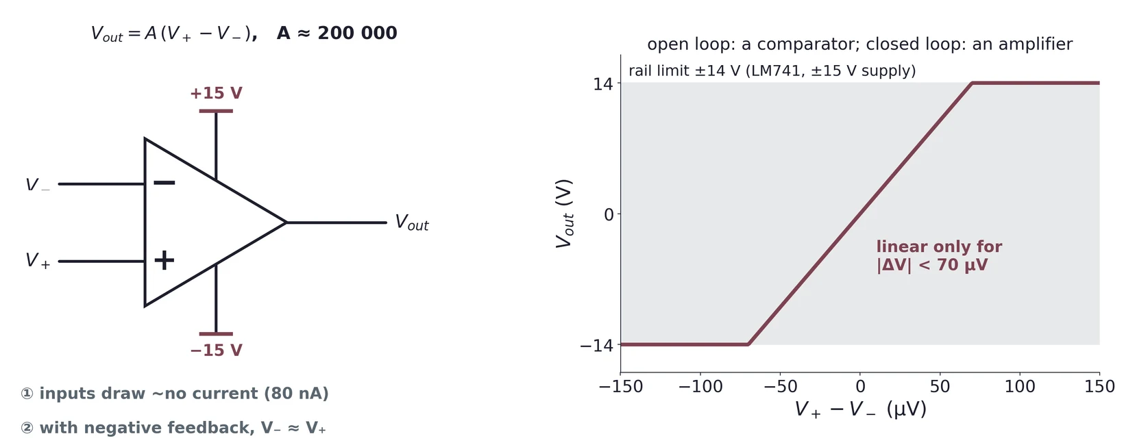
Open loop, 70 µV of difference already drives the output to a rail. With negative feedback the output settles where ; that is how every circuit in this lab works.
The LM741 on the bench
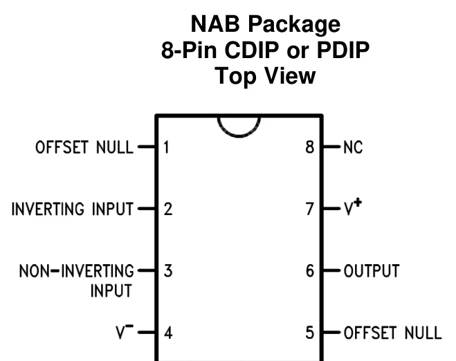
Pin 2: − input
Pin 3: + input
Pin 6: output
Pin 7: +15 V, pin 4: −15 V
Pins 1, 5: offset null (leave open)
What the LM741 can deliver
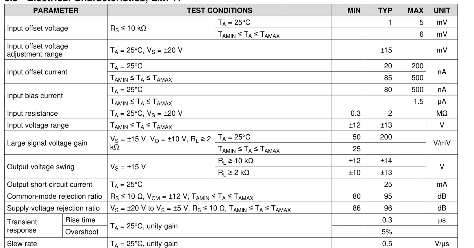
At ±15 V: output swings ±14 V into 10 kΩ, ±13 V into 2 kΩ; short-circuit current 25 mA; input bias 80 nA; slew rate 0.5 V/µs. These set every limit in Tasks 1.2 and 2.2.
A follower copies the voltage, adds current
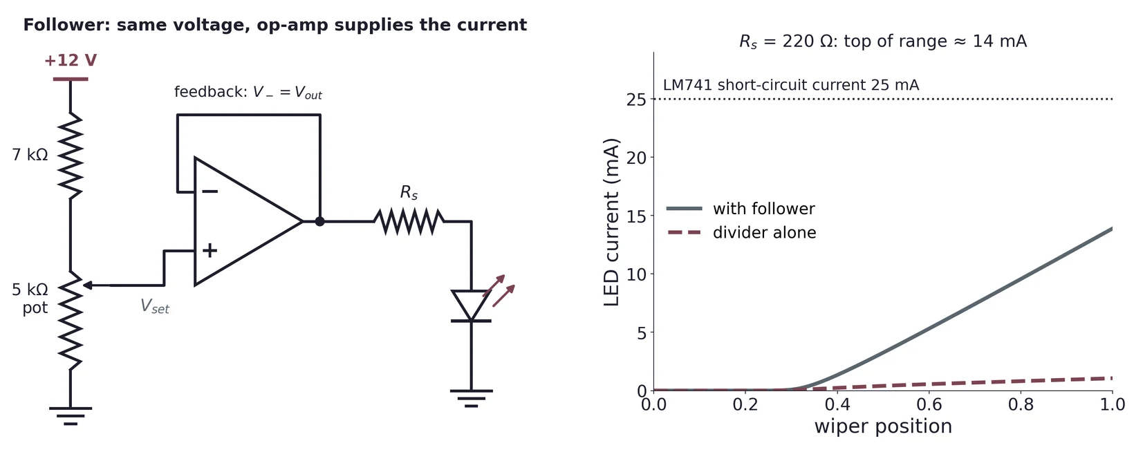
The + input draws 80 nA, so the divider stays at . The output drives the LED from the ±15 V supply: mA at the top of the range.
Put the LED inside the loop to fix the current
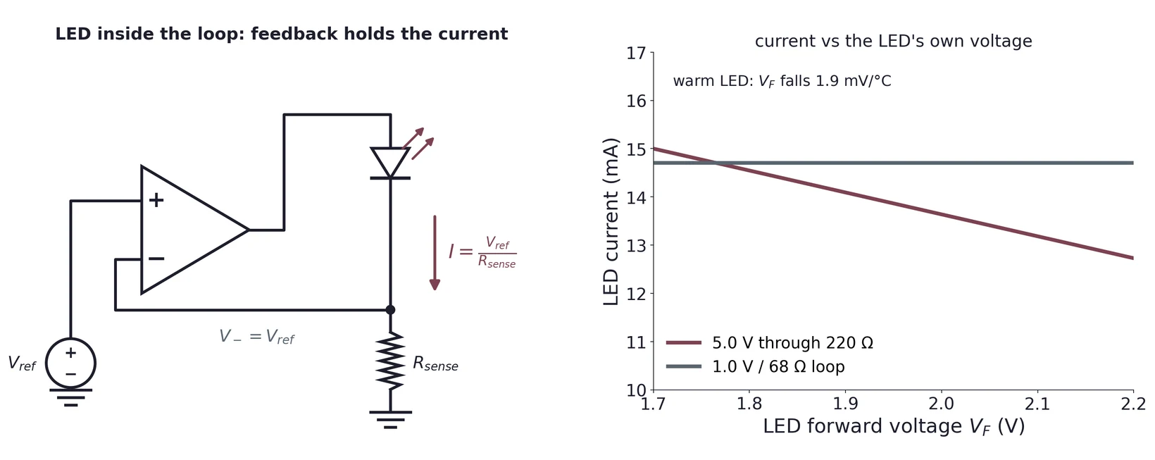
Feedback holds across , so whatever the LED's . Check the output: must stay below 14 V, and below 25 mA.
Part 3 · A photodiode: light in, current out
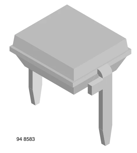
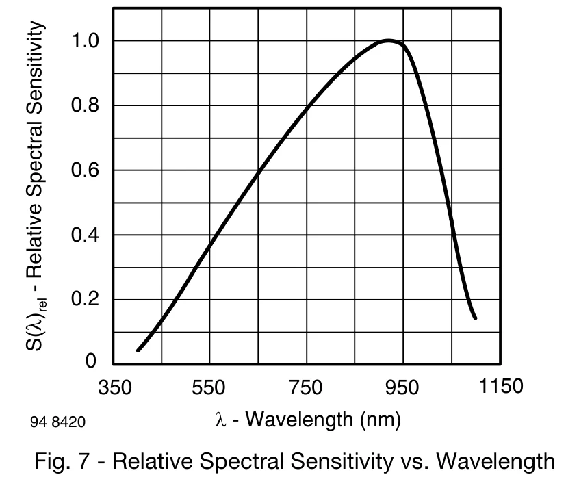
Vishay BPW34: sensitive 430–1100 nm, peak 900 nm. Each absorbed photon makes an electron–hole pair that the junction field sweeps apart: a current.
Model: a current source inside a diode
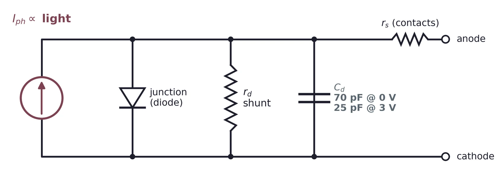
is the signal. The junction, and are what the circuit must work around. shrinks with reverse bias; it sets the speed.
Light shifts the I–V curve straight down
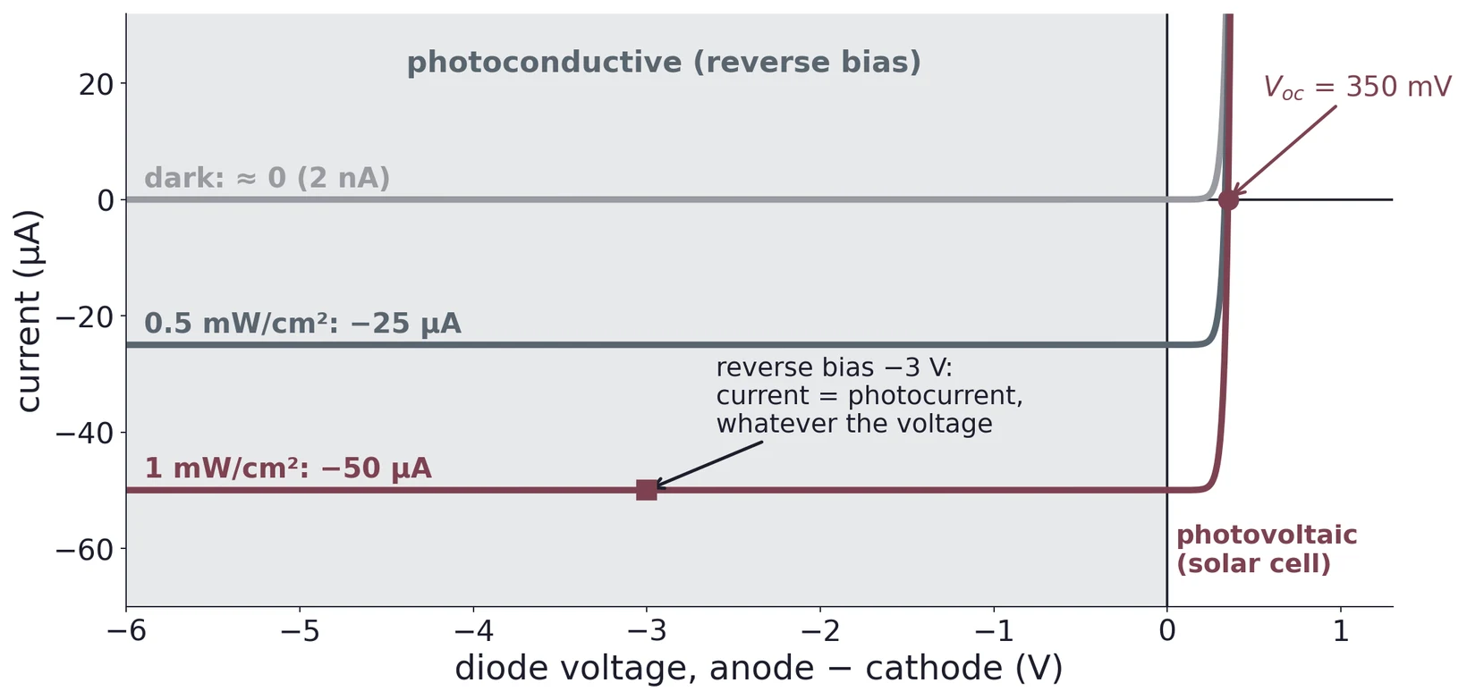
. In reverse bias the curves are flat: the current equals the photocurrent at any bias. That flat region is where a detector should sit.
Photocurrent is proportional to light
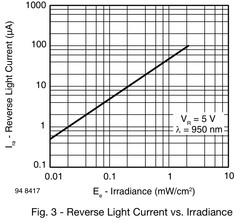
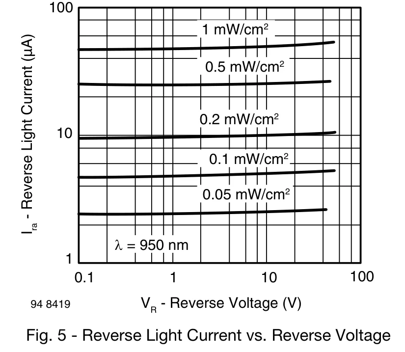
Left: a straight line over three decades, 50 µA at 1 mW/cm². Right: at fixed light, the current barely changes from 0.1 V to 50 V of reverse bias.
Reverse bias: faster, but with dark current
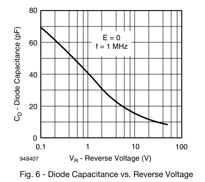
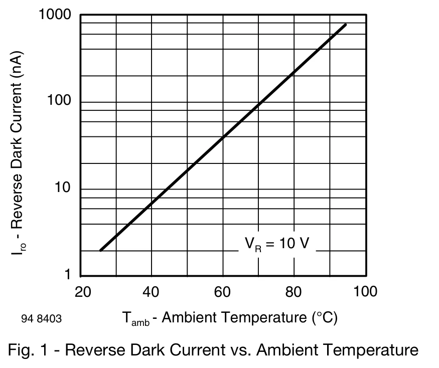
A wider depletion layer cuts from 70 pF at 0 V to 25 pF at 3 V. The price is leakage with no light: 2 nA at 10 V, doubling roughly every 8 °C.
The resistor detector
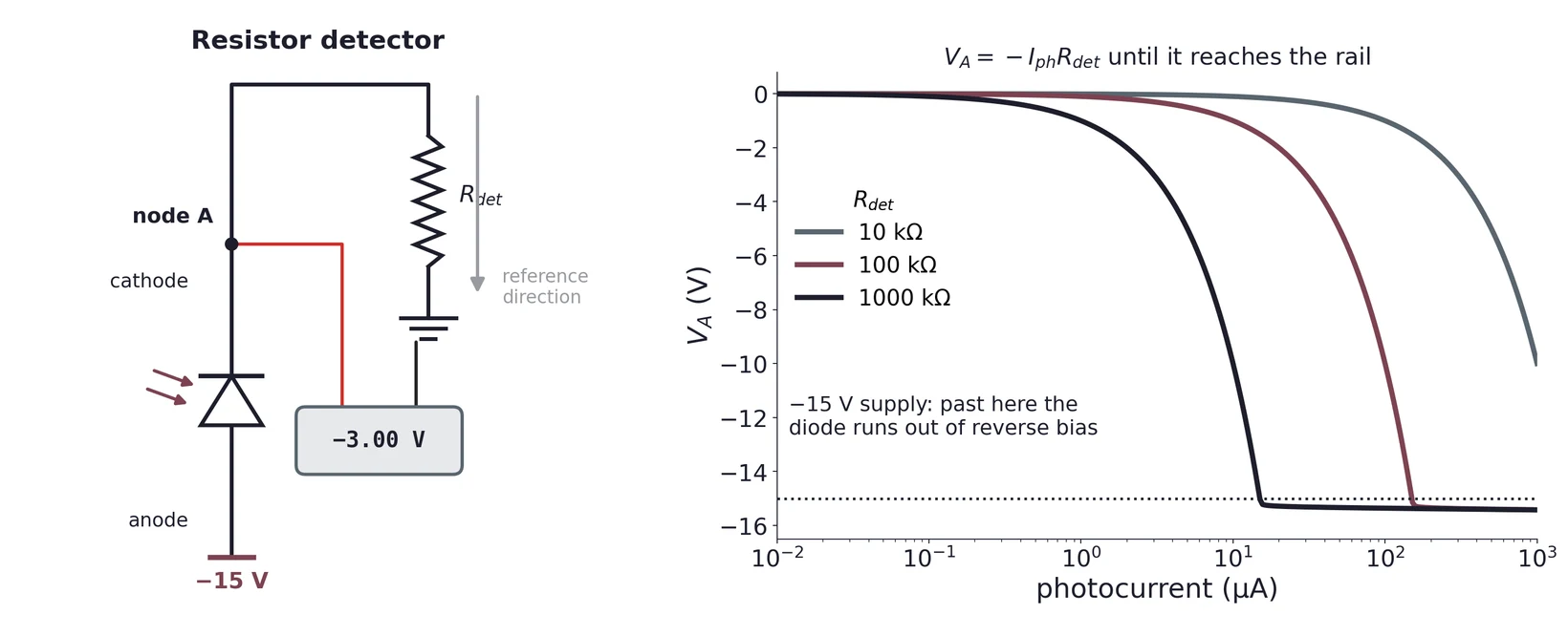
Photocurrent through gives . A bigger resistor gives more volts per µA, but can never pass the −15 V bias: the diode runs out of reverse voltage.
A negative reading is information
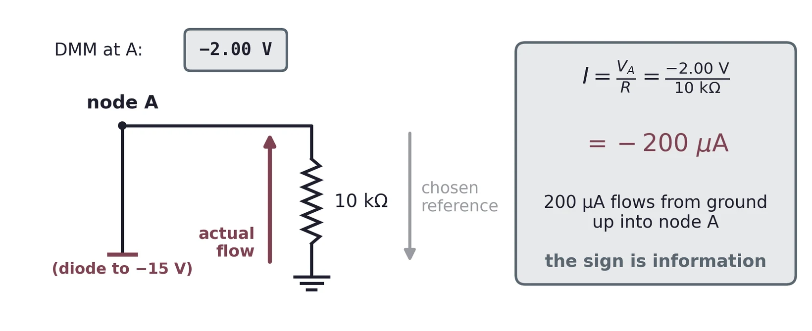
State the reference direction first, then divide. For Task 2, do the same with −3.0 V and your own resistor; the orientation of your diode decides the sign.
Part 4 · The TIA holds the diode at virtual ground
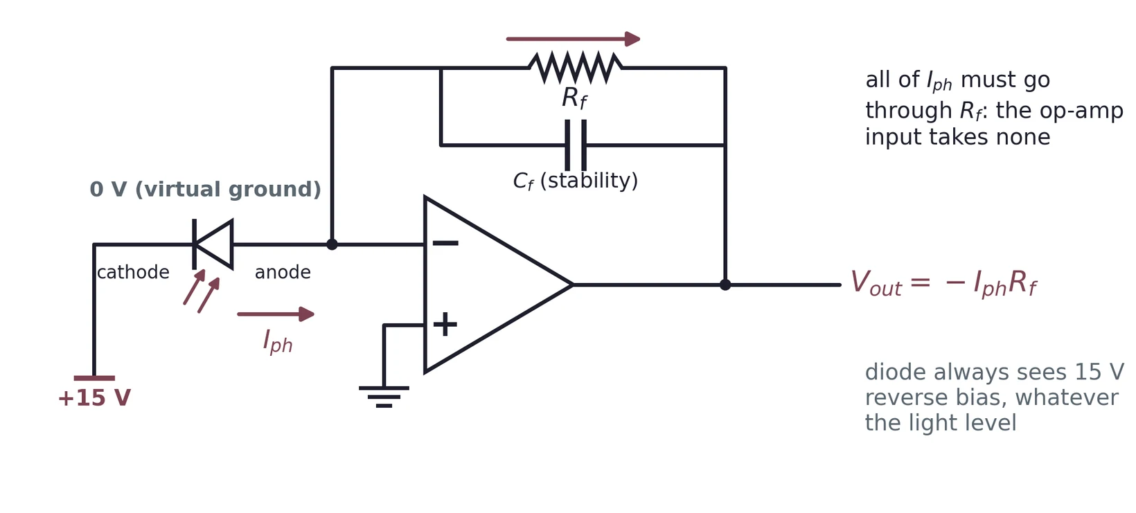
Feedback keeps the − input at 0 V, so the photocurrent has only one path: through . The output moves by ; with this orientation it goes negative.
Why the TIA beats the resistor
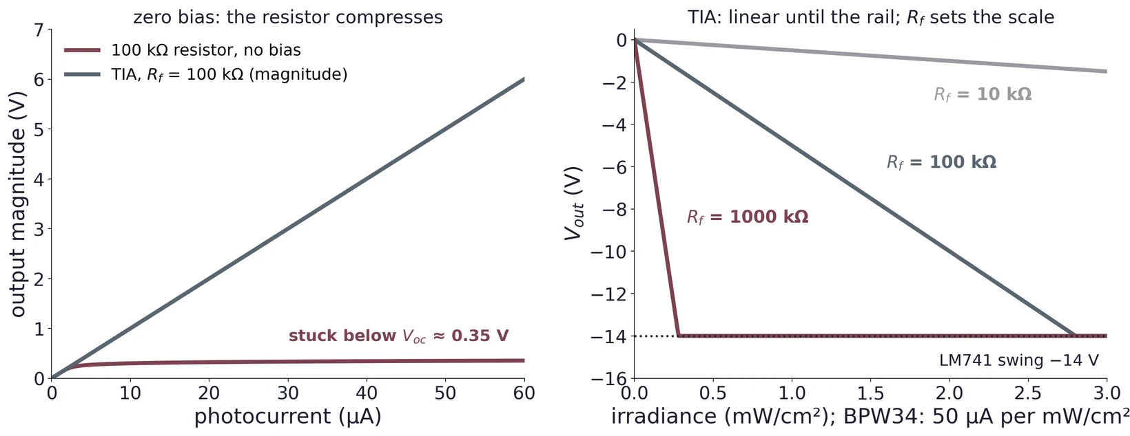
A resistor's voltage appears across the diode and eats its bias; at zero bias it stalls below 0.35 V. The TIA pins the diode voltage and stays linear to the rail.
Choose R_f from the brightest light
Full scale:
| V per µA | full scale | |
|---|---|---|
| 10 kΩ | 0.01 V | 1.4 mA |
| 100 kΩ | 0.1 V | 140 µA |
| 1 MΩ | 1 V | 14 µA |
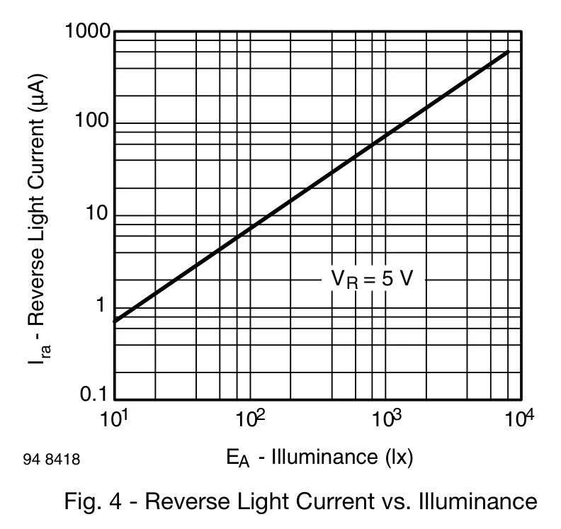
Office light, about 500 lx, gives about 40 µA (BPW34 Fig. 4): 4 V with 100 kΩ. Measure your brightest case first, then pick .
Diode capacitance limits bandwidth: add C_f
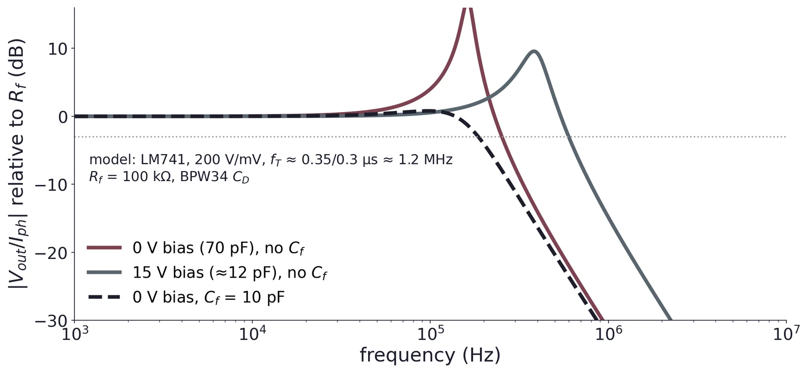
at the − input makes the loop ring. pF flattens it, with a corner at kHz. Reverse bias lowers and helps too.
Part 5 · Task 3: find the blocks first
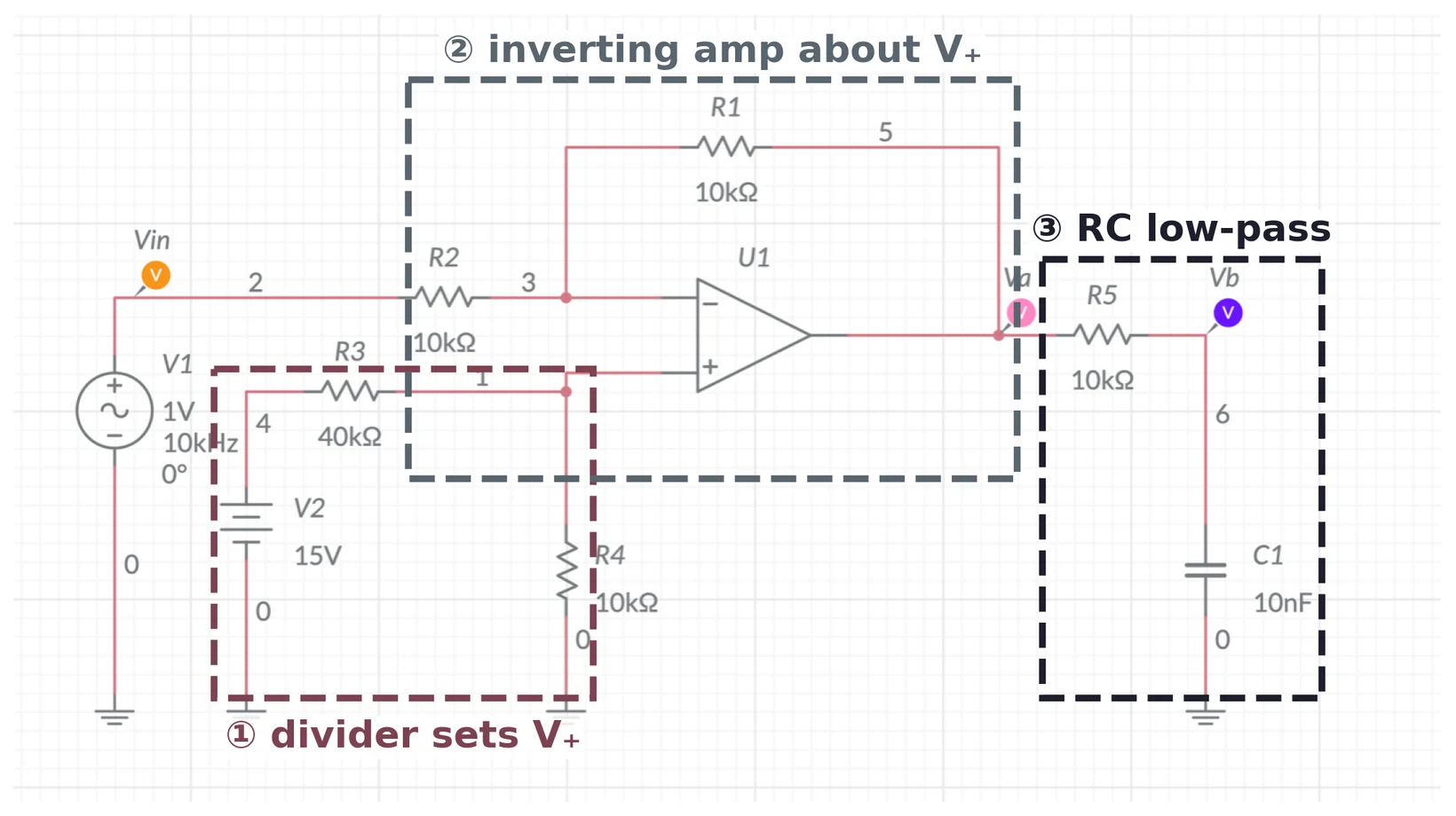
Name each block, solve it alone, then chain them. The divider fixes a DC level; the op-amp amplifies about it; R5 and C1 filter the result.
A biased inverting amplifier
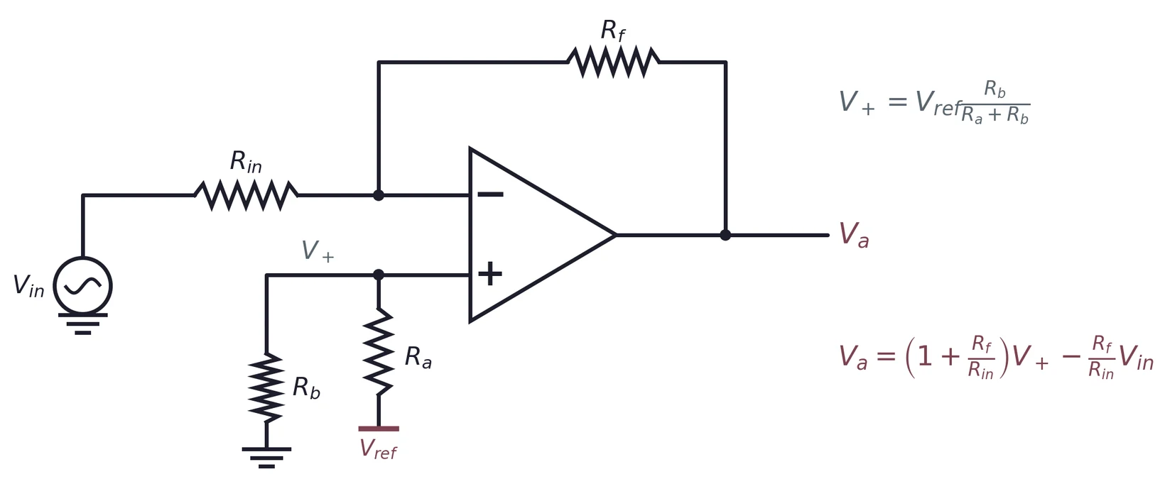
Superposition: alone sees gain ; alone sees the non-inverting gain . The inverting relation is measured from , not from ground.
The RC low-pass: smaller and later
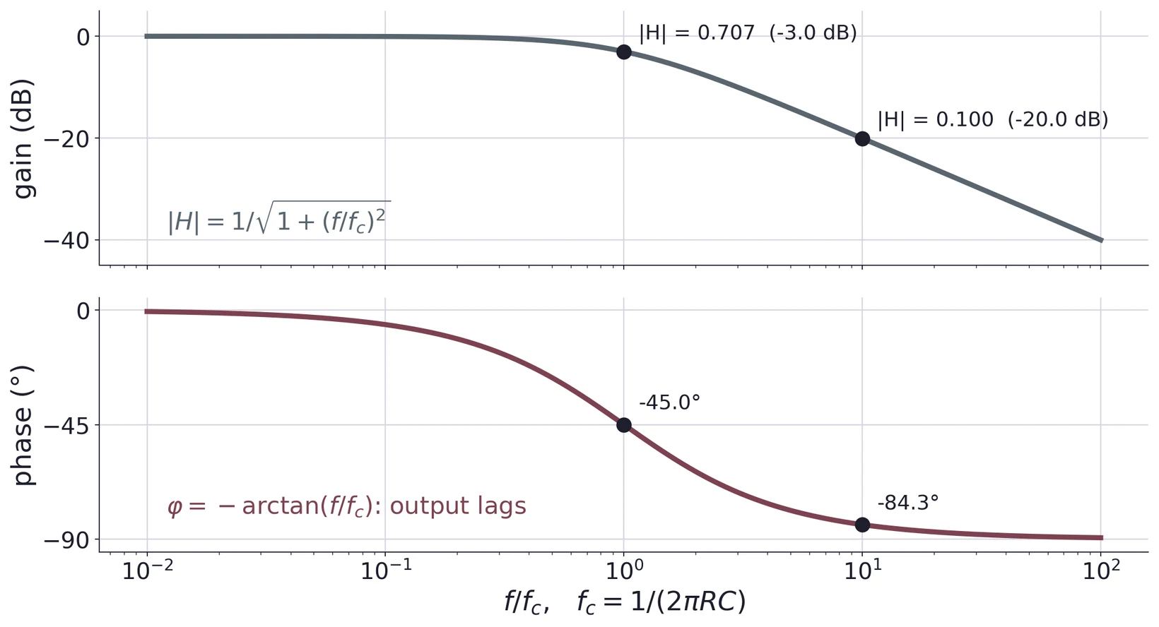
DC passes untouched (). Above the sine shrinks and lags, up to 90°. Compute both and at your frequency; the lag must show in your sketch.
Worked example with other values
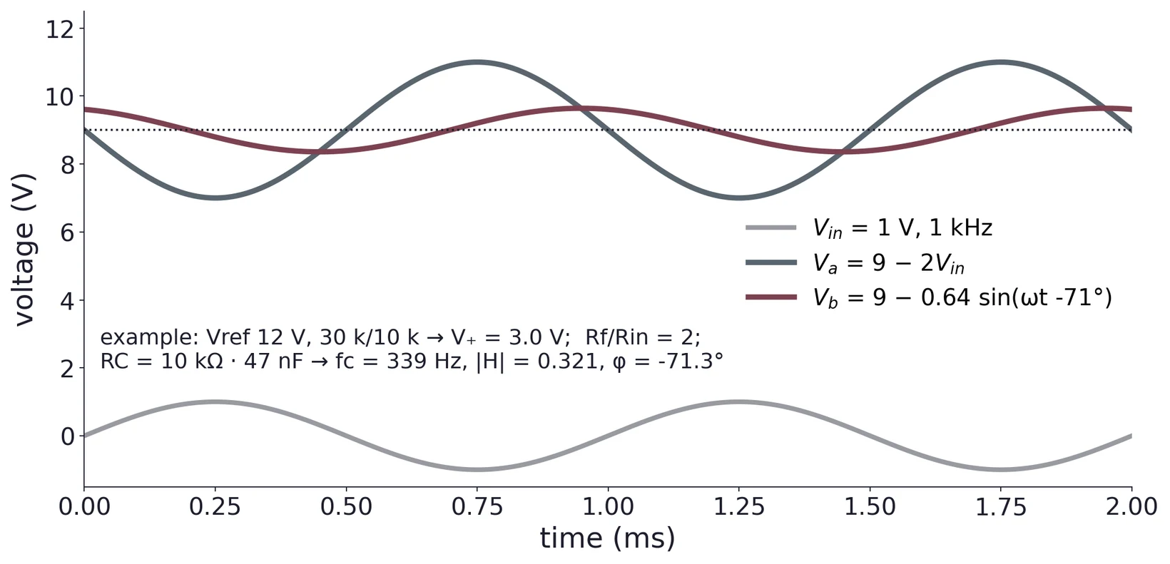
Not the Task 3 values. Here = 3.0 V, , and at 1 kHz ( = 2.95) the filter keeps 0.32 of the swing, 71° late. Your answer: same steps, your numbers, then a SPICE simulation.
Use ← → to move, Home / End to jump, and F for fullscreen.
Figure descriptions
Slide 2 · Part 1 · Lab 1: set a current, then read one
Lab 1 in three rows of blocks. Task 1, set a current: source limited to 5.0 V, current limit by resistor or op-amp, LED, light. Task 2, read a current: light, photodiode, resistor or TIA, DMM volts. Task 3, analyze a chain: sine in, biased inverting amplifier, RC low-pass, Va and Vb.
Slide 3 · An LED is a diode that emits light
Adafruit photograph of a clear through-hole LED showing its lens and two unequal-length leads.
Kingbright WP7113ID datasheet, relative intensity against wavelength: a single narrow peak labeled red near 627 nm, falling to zero by about 570 nm and 690 nm.
Slide 4 · Current rises exponentially with voltage
Kingbright WP7113ID datasheet curves at 25 °C. Left: forward current against forward voltage, near zero below 1.6 V and rising steeply to 20 mA at about 2.0 V. Right: luminous intensity rises in proportion to forward current from 0 to 20 mA.
Slide 5 · Read the limits before you design
Kingbright WP7113ID datasheet, absolute maximum ratings at 25 °C: power dissipation 75 mW, reverse voltage 5 V, junction temperature 125 °C, operating and storage temperature −40 to +85 °C, DC forward current 30 mA, peak forward current 160 mA at 1/10 duty cycle and 0.1 ms pulses.
Slide 6 · A series resistor turns a voltage into a current
Left: the LED current–voltage curve, modeled on the WP7113ID datasheet, crossed by dashed load lines of a 390 Ω resistor from 3, 5 and 9 V sources; the crossings give 3.1, 8.0 and 18.0 mA at about 1.8 to 2.0 V. Right: LED current against source voltage rises steadily with the 390 Ω resistor, reaching 25 mA at 12 V, but without a resistor it passes the 30 mA maximum at about 2.1 V.
Slide 8 · Adjustable but capped: a divider sets the top voltage
Left: a divider from +12 V through 7 kΩ and a 5 kΩ potentiometer sets V_set at most 5.0 V; the wiper feeds R_s and the LED to ground. Right: V_set against wiper position rises to 5.0 V with no load, but with 220 Ω and the LED attached it flattens near 1.9 V and the LED gets only 1.1 mA.
Slide 9 · Part 2 · The op-amp: huge gain, almost no input current
Left: an op-amp symbol with inputs V minus and V plus, output V_out, and ±15 V supplies; V_out = A(V+ − V−) with A about 200 000; inputs draw almost no current (80 nA) and with negative feedback V− ≈ V+. Right: open-loop output against the input difference, linear only between about −70 and +70 µV and clipped at ±14 V.
Slide 10 · The LM741 on the bench
TI LM741 datasheet, NAB 8-pin CDIP or PDIP package, top view: pin 1 offset null, 2 inverting input, 3 non-inverting input, 4 V minus, 5 offset null, 6 output, 7 V plus, 8 no connection.
Slide 11 · What the LM741 can deliver
TI LM741 datasheet section 6.5, electrical characteristics: input offset voltage 1 mV typical, 5 mV maximum; input bias current 80 nA typical; large-signal voltage gain 200 V/mV typical at ±15 V; output voltage swing ±14 V typical into 10 kΩ and ±13 V into 2 kΩ; output short-circuit current 25 mA; common-mode rejection 95 dB; rise time 0.3 µs; slew rate 0.5 V/µs.
Slide 12 · A follower copies the voltage, adds current
Left: the 12 V divider's wiper drives the non-inverting input of an op-amp wired as a follower, whose output drives R_s and the LED. Right: LED current against wiper position reaches about 14 mA with the follower, compared with about 1 mA from the divider alone, below the LM741's 25 mA short-circuit limit.
Slide 13 · Put the LED inside the loop to fix the current
Left: an op-amp current regulator: V_ref on the non-inverting input; the output drives the LED, whose cathode meets R_sense to ground and feeds back to the inverting input, so V− = V_ref and I = V_ref/R_sense. Right: LED current against forward voltage from 1.7 to 2.2 V: 5.0 V through 220 Ω falls from 15 to 12.7 mA, while a 1.0 V over 68 Ω loop holds 14.7 mA.
Slide 14 · Part 3 · A photodiode: light in, current out
Vishay BPW34 datasheet drawing: a small flat rectangular photodiode package with a clear top window and two leads.
Vishay BPW34 datasheet Fig. 7: relative spectral sensitivity against wavelength, rising from near zero at 400 nm to a peak near 900 nm and falling steeply to about 0.15 at 1100 nm.
Slide 15 · Model: a current source inside a diode
Photodiode equivalent circuit: a light-controlled current source I_ph in parallel with the junction diode, a shunt resistance r_d and the capacitance C_d, 70 pF at 0 V and 25 pF at 3 V for the BPW34, with a small series contact resistance r_s to the anode terminal; the cathode is the lower terminal.
Slide 16 · Light shifts the I–V curve straight down
Photodiode current against voltage for dark, 0.5 and 1 mW/cm²: the curves are flat in the shaded reverse-bias region at about 0, −25 and −50 µA, and rise steeply in forward bias; the brightest curve crosses zero at the open-circuit voltage of 350 mV in the photovoltaic quadrant. A marker at −3 V notes that the current equals the photocurrent whatever the voltage.
Slide 17 · Photocurrent is proportional to light
Vishay BPW34 datasheet Fig. 3: reverse light current against irradiance on log–log axes at 5 V and 950 nm, a straight line from about 0.5 µA at 0.01 mW/cm² to about 100 µA at 2 mW/cm².
Vishay BPW34 datasheet Fig. 5: reverse light current against reverse voltage from 0.1 to 50 V for irradiances from 0.05 to 1 mW/cm², each curve nearly flat, about 50 µA at 1 mW/cm².
Slide 18 · Reverse bias: faster, but with dark current
Vishay BPW34 datasheet Fig. 6: diode capacitance in the dark at 1 MHz against reverse voltage, falling from about 70 pF at 0.1 V to about 25 pF at 3 V and below 10 pF near 50 V.
Vishay BPW34 datasheet Fig. 1: reverse dark current at 10 V against ambient temperature on a log scale, rising in a straight line from about 2 nA at 25 °C to about 800 nA at 95 °C.
Slide 19 · The resistor detector
Left: a resistor detector with the photodiode anode at −15 V and cathode at node A, R_det from node A to ground, and a DMM reading −3.00 V at node A. Right: node voltage V_A against photocurrent on a log scale for 10 kΩ, 100 kΩ and 1 MΩ: each follows V_A = −I_ph R_det, then stops near −15.4 V where the diode runs out of reverse bias.
Slide 20 · A negative reading is information
Worked sign example: node A connects to a 10 kΩ resistor to ground and the DMM reads −2.00 V. The chosen reference direction points down through the resistor, while the actual current flows up. I = V_A/R = −2.00 V/10 kΩ = −200 µA: 200 µA flows from ground up into node A.
Slide 21 · Part 4 · The TIA holds the diode at virtual ground
Transimpedance amplifier: the photodiode cathode is at +15 V and its anode at the op-amp inverting input, held at 0 V virtual ground; the non-inverting input is grounded; R_f with C_f in parallel runs from the output back to the inverting input. The photocurrent flows through R_f, so V_out = −I_ph R_f, and the diode always sees 15 V of reverse bias.
Slide 22 · Why the TIA beats the resistor
Left: output magnitude against photocurrent from 0 to 60 µA: a 100 kΩ resistor with no bias compresses below about 0.35 V, while a TIA with 100 kΩ rises linearly to 6 V. Right: TIA output against irradiance for R_f 10 kΩ, 100 kΩ and 1 MΩ, falling linearly until the LM741's −14 V swing, reached at 0.28 mW/cm² for 1 MΩ and 2.8 mW/cm² for 100 kΩ.
Slide 23 · Choose R_f from the brightest light
Vishay BPW34 datasheet Fig. 4: reverse light current at 5 V against illuminance on log–log axes, a straight line from about 0.7 µA at 10 lx through about 7 µA at 100 lx and 75 µA at 1000 lx to about 600 µA at 8000 lx.
Slide 24 · Diode capacitance limits bandwidth: add C_f
Modeled TIA response relative to R_f against frequency for an LM741 with R_f = 100 kΩ: with the BPW34 at 0 V (70 pF) and no C_f it peaks sharply near 160 kHz; at 15 V bias (about 12 pF) it peaks near 400 kHz; with C_f = 10 pF the 70 pF case is flat and falls through −3 dB near 170 kHz.
Slide 25 · Part 5 · Task 3: find the blocks first
The Lab 1 Task 3 Multisim schematic with three dashed boxes: the 15 V source and the R3–R4 divider labeled 1, divider sets V plus; R2, R1 and the op-amp labeled 2, inverting amplifier about V plus; R5 and C1 labeled 3, RC low-pass, between Va and Vb.
Slide 26 · A biased inverting amplifier
A biased inverting amplifier: V_in drives the inverting input through R_in, R_f feeds back from output V_a, and the non-inverting input sits at V plus from a divider R_a from V_ref and R_b to ground. V+ = V_ref R_b/(R_a + R_b) and V_a = (1 + R_f/R_in)V+ − (R_f/R_in)V_in.
Slide 27 · The RC low-pass: smaller and later
First-order low-pass response against f/f_c from 0.01 to 100: gain is 0 dB at low frequency, −3 dB (|H| = 0.707) at f_c and −20 dB (0.100) at 10 f_c; phase goes from 0 to −45 degrees at f_c and −84.3 degrees at 10 f_c, approaching −90 degrees.
Slide 28 · Worked example with other values
Worked example with its own values, not the Task 3 values: over 2 ms, V_in is a 1 V, 1 kHz sine; V_a = 9 − 2V_in swings between 7 and 11 V, inverted; V_b = 9 − 0.64 sin(ωt − 71°) is a smaller sine about 9 V, lagging. V_ref 12 V with 30 k and 10 k gives V+ = 3.0 V; RC = 10 kΩ × 47 nF gives f_c = 339 Hz, |H| = 0.321, φ = −71.3°.