1 Where Lab 1 Sits
Lab 1 is entirely analog. The hardware decides everything: a resistor sets a current, a feedback loop sets a gain, a filter sets a bandwidth. There is no software, and that is on purpose. From Lab 3 on, a Raspberry Pi makes the decisions, and you will want a firm grip on what the analog circuitry is doing before you connect a computer to it.
The first two tasks are both about current. An LED must be fed a controlled current; a photodiode produces a small current that must be read. The first tool for each job is a resistor, and the second is an op-amp with negative feedback.
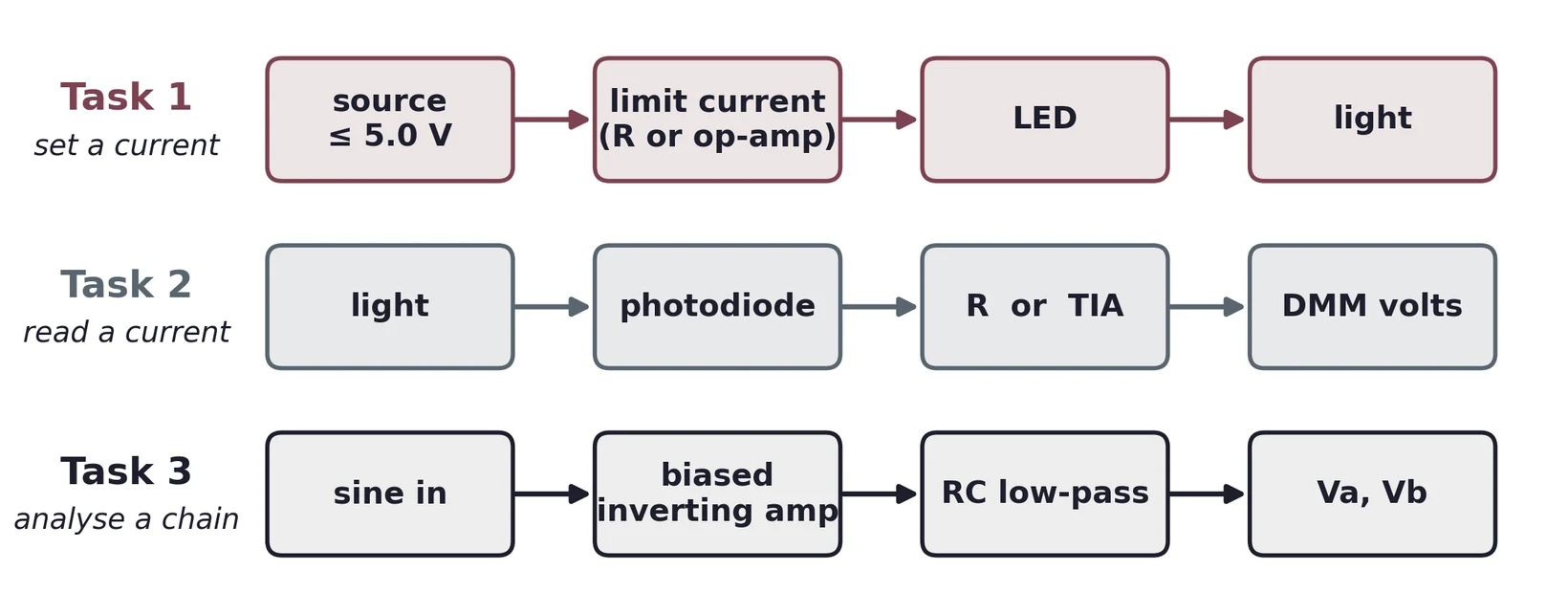
A measurement chain is a sequence of deliberate conversions: voltage to current in the LED driver, light to current in the photodiode, current to voltage in the detector. At each step you choose a component value that makes the next step well behaved. Design from the quantity you want to end up with, and work backwards.
1.1 Task map
| Lab 1 task | What you build | Concept & section |
|---|---|---|
| 1.1 | Adjustable LED driver, at most 5.0 V applied, current limited | The LED; series limiting; the capped divider (§2–4) |
| 1.2 | The same driver built around an op-amp | Op-amp rules; follower and current regulator (§5–6) |
| 2.1 | Photodiode and resistor light detector; the current for a −3.0 V reading | Photodiode model, reverse bias, sign conventions (§7–8) |
| 2.2 | Photodiode with an op-amp; the current for a −3.0 V reading | Transimpedance amplifier (§9) |
| 3 | Analyze the given op-amp circuit; find Va and Vb; sketch and simulate | Biased inverting stage plus RC low-pass (§10) |
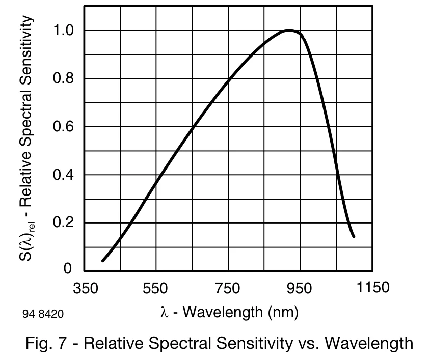
The parts named in these notes (a Kingbright WP7113ID red LED, a TI LM741 op-amp, a Vishay BPW34 photodiode) are typical examples of each kind of part, and your kit may hold different ones. Look up the datasheet of each part you actually use, or measure it, and use those numbers in your report.
2 The LED
2.1 A diode that emits light
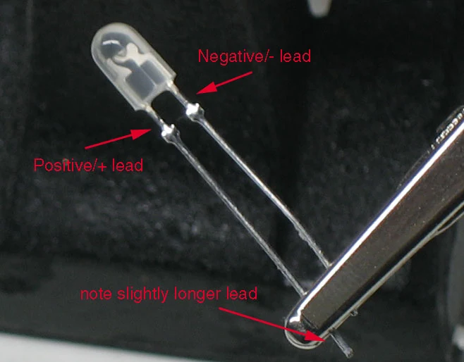
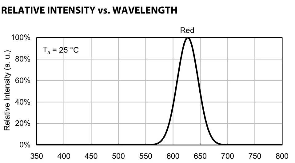
A light-emitting diode is a PN junction made from a semiconductor whose band gap matches the energy of a visible photon. Under forward bias, electrons from the N side and holes from the P side meet in the junction and recombine; each recombination can release the gap energy as one photon. The color is therefore set by the material: the WP7113ID is gallium arsenide phosphide on gallium phosphide, with a peak at 627 nm.
2.2 Current rises exponentially with voltage
Like any diode, the LED obeys (approximately) the Shockley law,
with mV at room temperature and an ideality factor between 1 and 3. The consequence is the whole reason for Task 1: near the forward voltage, a small change in voltage makes a large change in current.
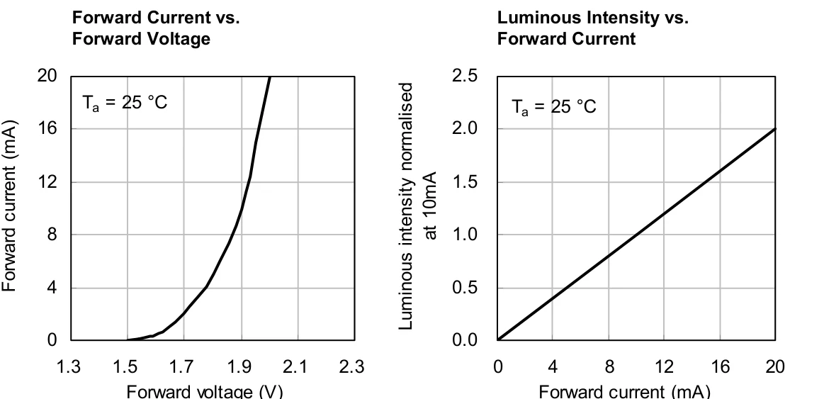
Two conclusions follow from Figure 4. Brightness follows current, not voltage, so the quantity to control is current. And a voltage source cannot control it: between 1.7 and 2.0 V the current multiplies by five, and the forward voltage itself falls by about 1.9 mV for every degree the LED warms. Connect an LED straight across an adjustable voltage source and the current is at the mercy of millivolts. Worse, as the LED heats up its forward voltage drops, so the current climbs, so it heats up more. That loop is called thermal runaway, and it ends with a dead LED.
2.3 Read the limits before you design
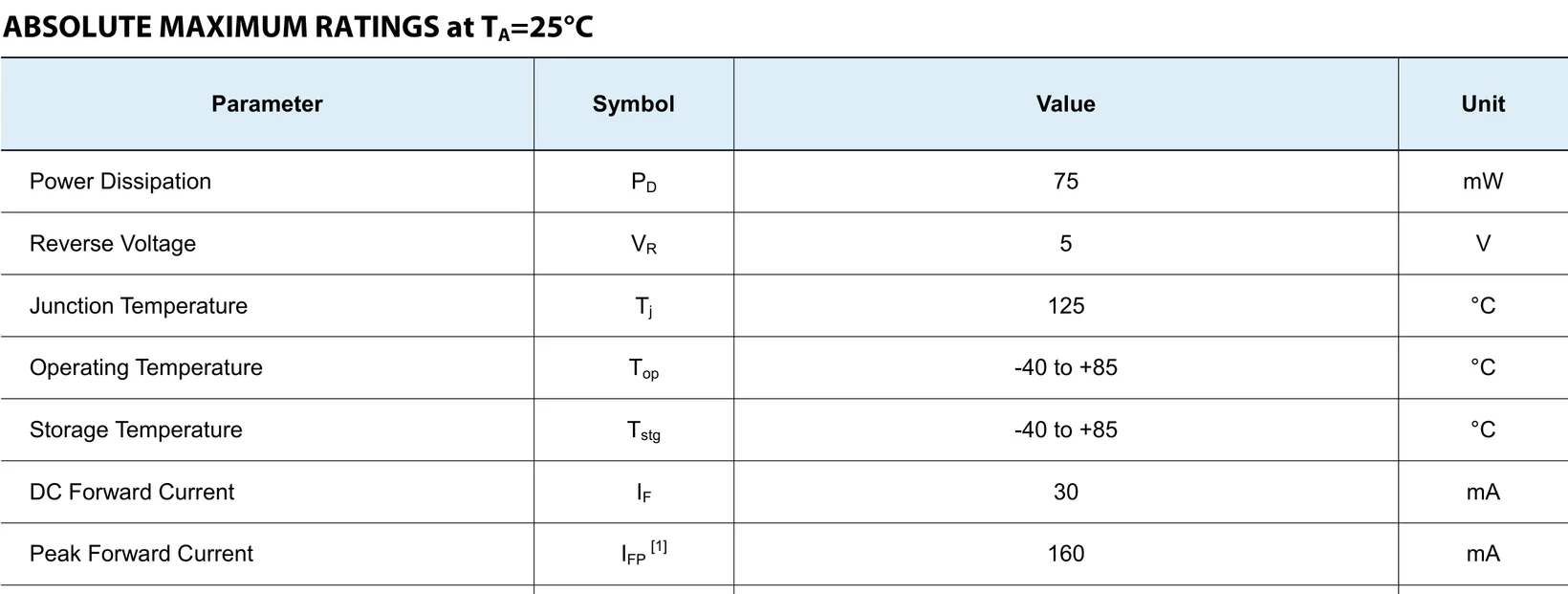
| Datasheet value | WP7113ID | What it means for the driver |
|---|---|---|
| Forward voltage at 10 mA | 1.9 V typ, 2.3 V max | Parts vary. No minimum is given, so for the current limit assume a little below typical (§3.2 uses 1.8 V) |
| DC forward current | 30 mA max | Design for well below it, 10–20 mA |
| Power dissipation | 75 mW max | must stay below it |
| Reverse voltage | 5 V max | Never connect the LED backwards across a supply |
3 The Series Resistor
3.1 The load line
Put a resistor in series with the LED and drive the pair from a source . Kirchhoff's voltage law gives one equation, , which is a straight line in the LED's current–voltage plane: the load line . The LED's own curve is a second relation. The operating point is where they cross.
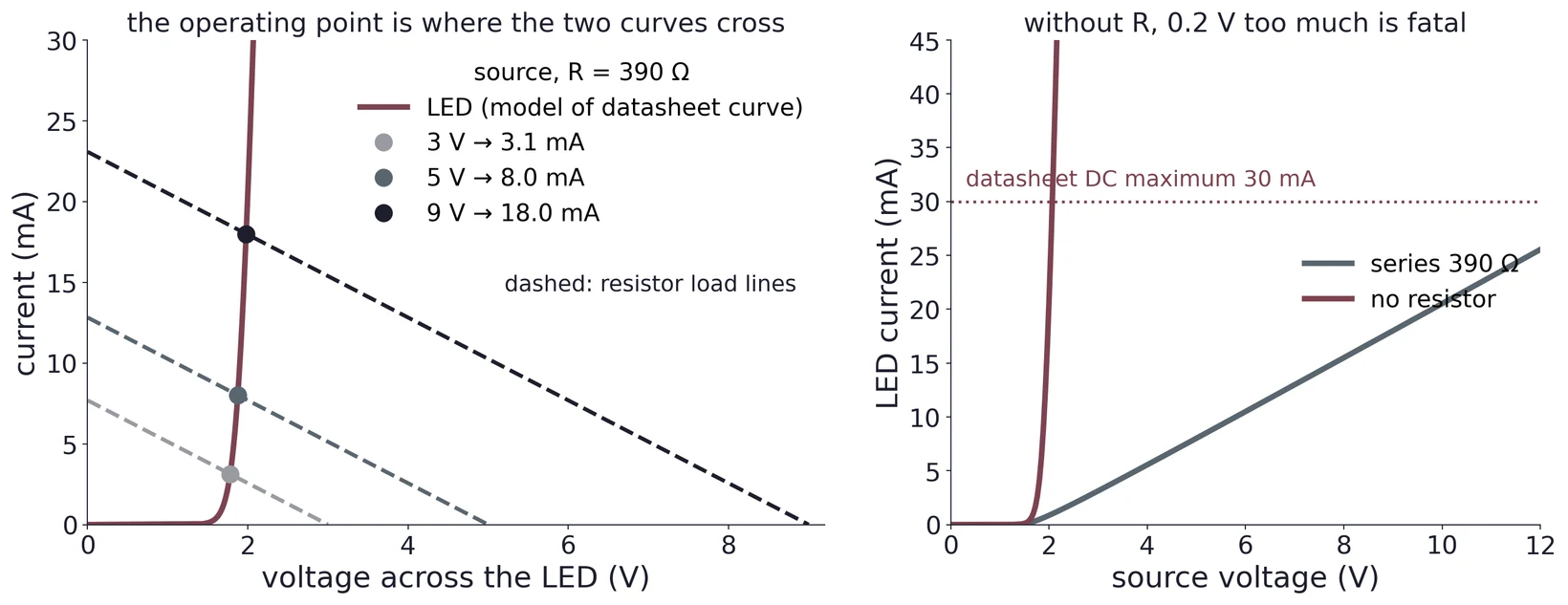
Because the LED voltage barely moves once it conducts, the current is set almost entirely by the resistor:
3.2 Design for the worst case
Design from the current limit, at the worst case: the highest source voltage your adjustment allows and the lowest forward voltage the LED might have.
The datasheet gives only a typical (1.9 V) and a maximum forward voltage, so take = 1.8 V, a little below typical. With = 9.0 V and = 20 mA, Equation (3) gives . If your kit has no 360 Ω resistor, round up, never down. Here are the neighboring values, checked for current and for power in both parts:
| R | I at 9 V | P in R = I²R | P in LED |
|---|---|---|---|
| 330 Ω | 21.8 mA (too high) | 0.16 W | 39 mW |
| 390 Ω | 18.5 mA | 0.13 W | 33 mW |
| 470 Ω | 15.3 mA | 0.11 W | 28 mW |
330 Ω breaks the 20 mA limit, so it is out. 390 Ω keeps the current under 20 mA. It dissipates 0.13 W, so a ¼ W resistor runs at about half its rating, which is a comfortable margin. The LED dissipates 33 mW of its 75 mW allowance.
4 Adjustable and Capped: the Divider
4.1 Read the requirement carefully
Task 1.1 asks you to limit the voltage applied to the LED to 5.0 V and to include current limiting. Those are separate requirements with separate reasoning: one about the largest node voltage your adjustment can produce, one about the largest current at that setting. A design that meets only one of them is incomplete.
What does "the voltage applied to the LED" mean? Once it conducts, the LED itself only ever has about 2 V across it, so the sensible reading is the adjustable drive voltage that feeds the LED and its series resistor ( in Figure 7). Whatever you decide, name the node in your report and show that it cannot go above 5.0 V.
The simplest way to get an adjustable voltage with a hard ceiling is a potentiometer below a fixed resistor. The two form a divider, and the wiper picks off part of the pot's share. With the wiper at the top you get the most:
No setting of the knob can exceed that value. For example, from a 12 V supply a 7 kΩ resistor above a 5 kΩ pot gives V at most.
4.2 A loaded divider sags
Equation (4) is true only when nothing draws current from the wiper. An LED branch draws milliamps, and the divider has its own source resistance. Seen from the wiper at the top of its travel, the divider is a Thévenin source of 5.0 V behind kΩ. That 2.9 kΩ is in series with and the LED. It is far larger than any sensible , so it ends up setting the current.
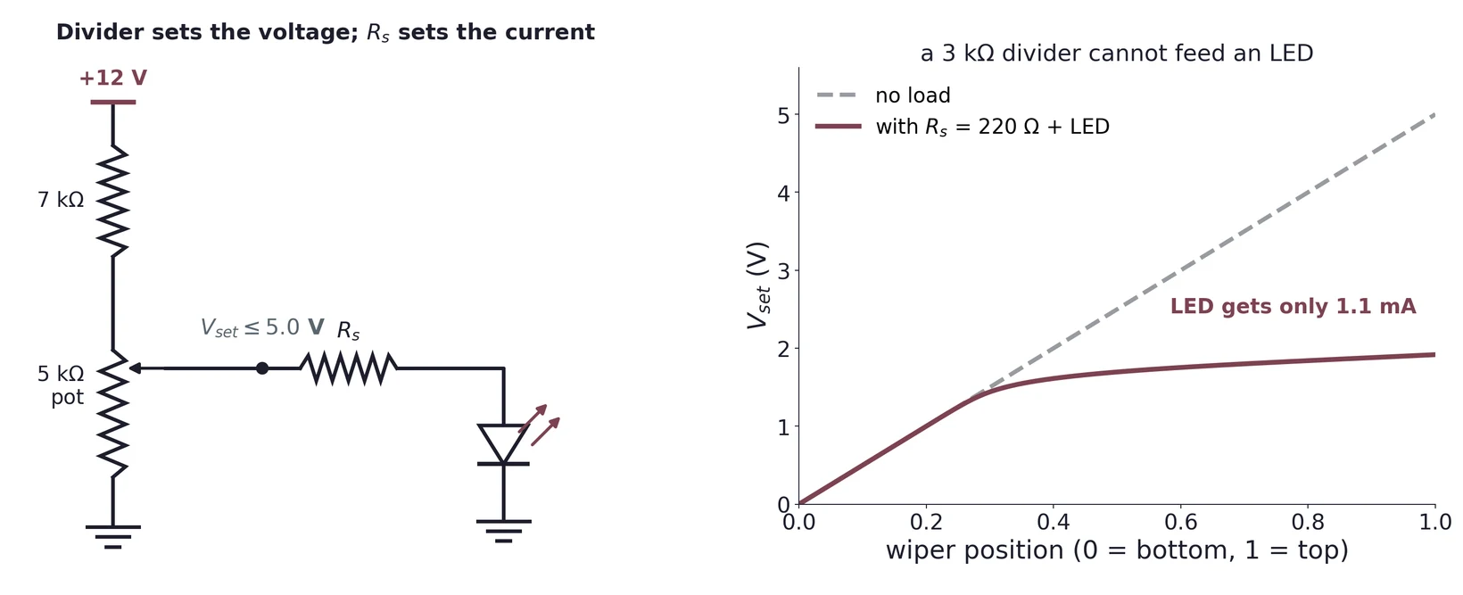
The fix is either a much stiffer divider (small resistors, wasting current and power in the divider) or a buffer that copies the divider's voltage without loading it. The second is Task 1.2.
(a) A supply adjusts from 0 to 12 V and the LED has = 2.0 V. Choose a series resistor so the current never exceeds 15 mA, and state the current at the top of the range.
(b) For that same resistor, what is the current at 4 V? Comment on how linearly the brightness follows the knob.
(c) Redesign the 12 V divider of §4.1 with a 500 Ω pot. What fixed resistor keeps the maximum at 5.0 V unloaded, how much current does the divider waste, and roughly how far does it sag with a 20 mA load?
5 The Op-Amp
5.1 Huge gain, almost no input current
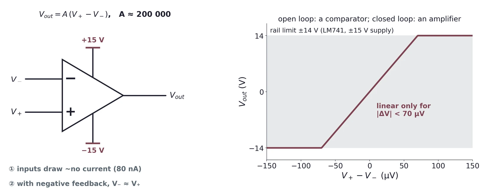
An op-amp amplifies the difference between its two inputs by an enormous factor:
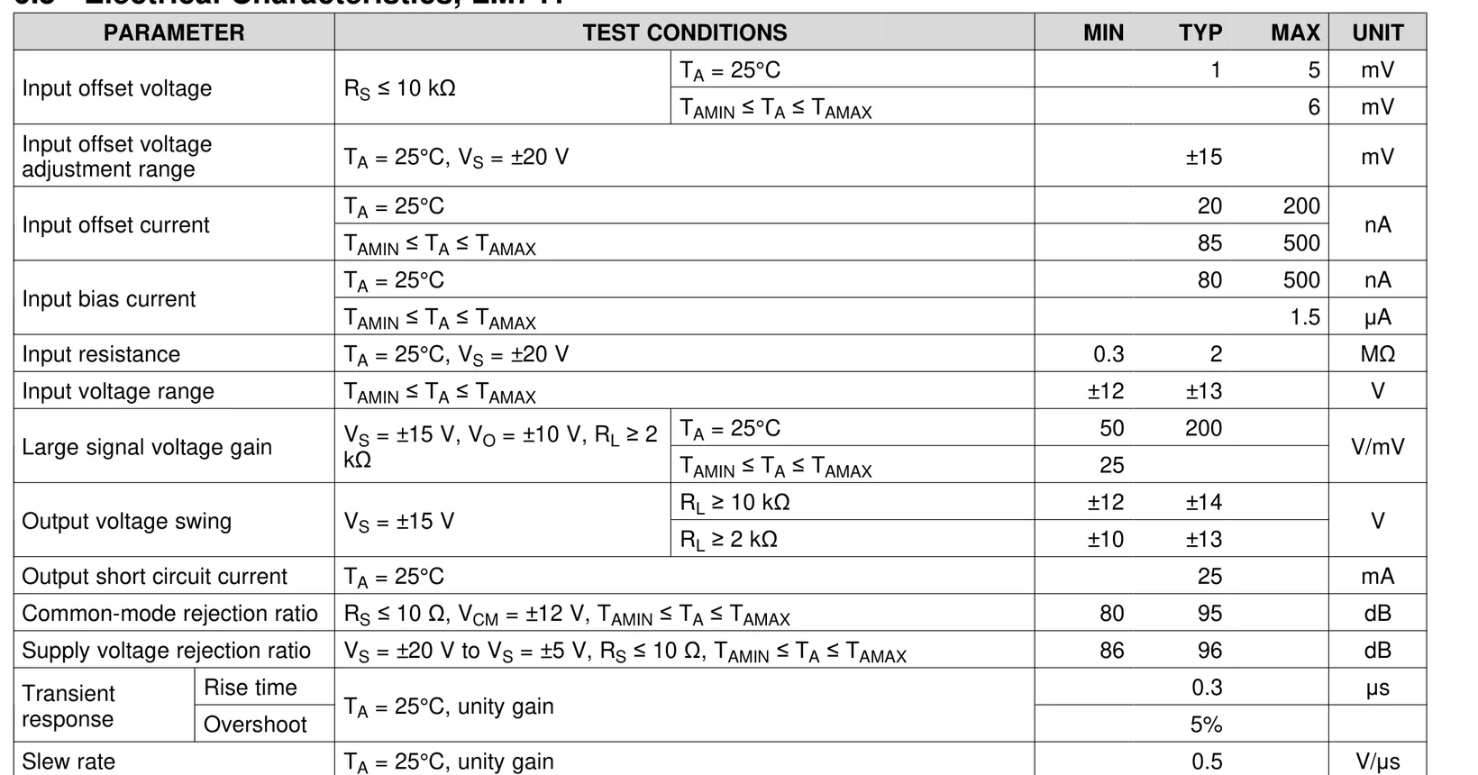
The output can swing only about ±14 V, so the input difference that keeps it off the rails is tiny: µV. Without feedback, the op-amp simply slams to one rail or the other, like a comparator. With negative feedback, part of the output is returned to the inverting input; if the output rises, rises and pulls it back. The loop settles where . Together with the tiny input current, that gives the two working rules for every op-amp circuit in this lab:
- No current into the inputs. The LM741's input bias current is 80 nA typical, small next to the microamps and milliamps in this lab.
- With negative feedback, .
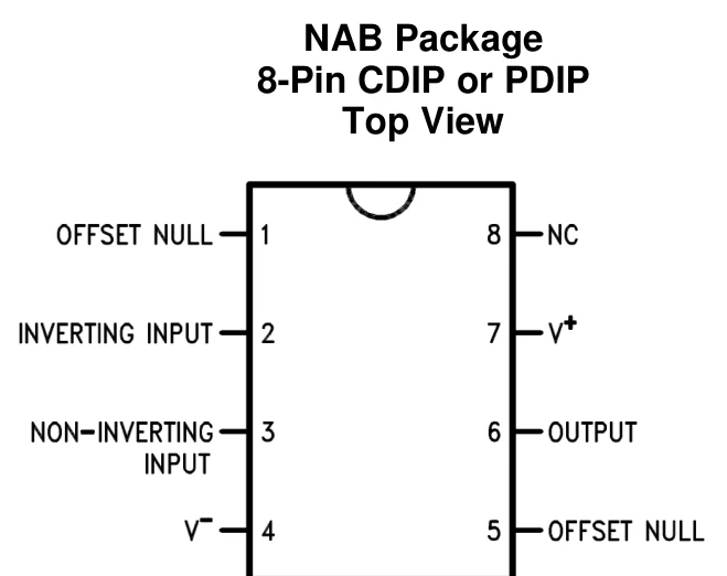
5.2 The LM741
| LM741 limit | Value (±15 V) | Where it bites in Lab 1 |
|---|---|---|
| Output swing | ±13 to ±14 V | Largest TIA output; largest drive voltage for an LED |
| Output current | 25 mA (short circuit) | Largest LED current the op-amp can deliver |
| Bandwidth | ≈ 0.35/0.3 µs ≈ 1.2 MHz | TIA speed and stability (§9.3) |
| Slew rate | 0.5 V/µs | A 10 V step takes at least 20 µs |
6 Op-Amp LED Drivers
6.1 The follower
Connect the output straight to the inverting input and feed to the non-inverting input. Rule 2 gives : a voltage follower. Rule 1 says the divider now supplies almost nothing, so it no longer sags; the LED current comes from the op-amp's supply instead.
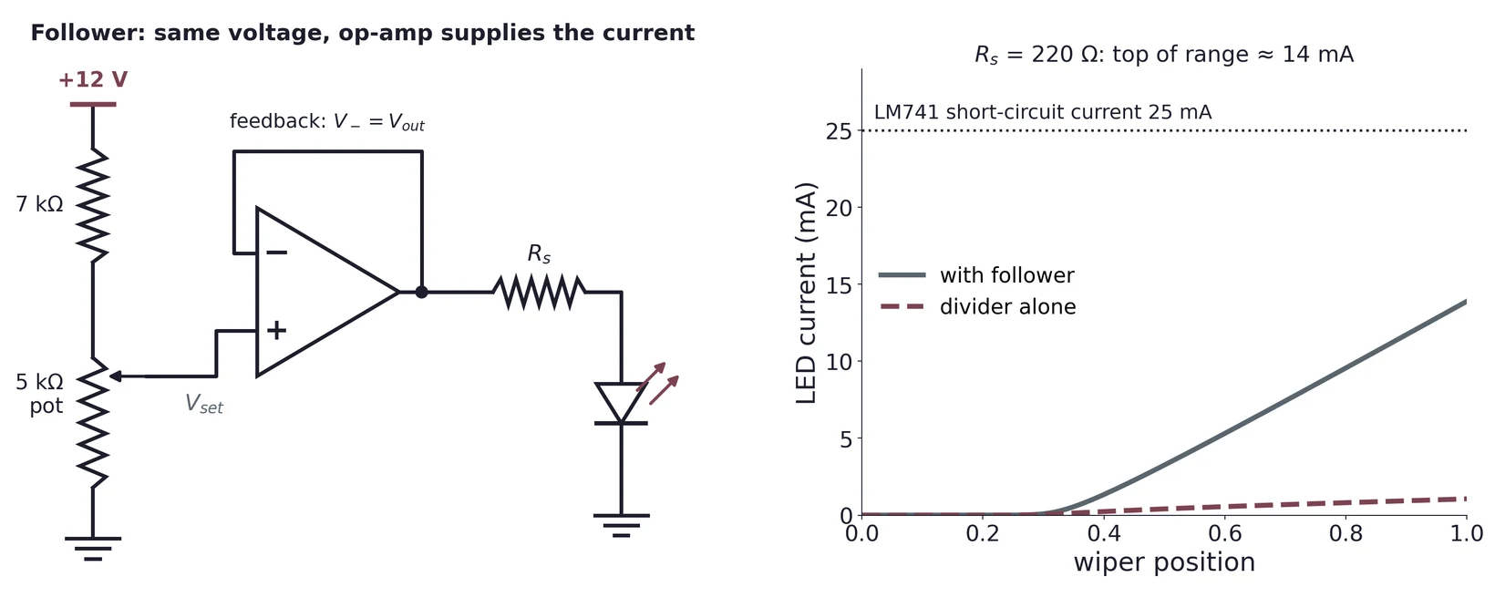
With = 5.0 V, = 1.9 V and = 220 Ω the top current is mA. The 5.0 V cap now holds at the op-amp output too, because the output follows .
6.2 The LED inside the loop
A follower still sets a voltage and lets Equation (2) decide the current, so the current still depends on . Put the LED inside the feedback loop instead, with a sense resistor from the LED's cathode to ground, and feed the node between them back to the inverting input. Rule 2 forces , so the voltage across is fixed, and so is the current:
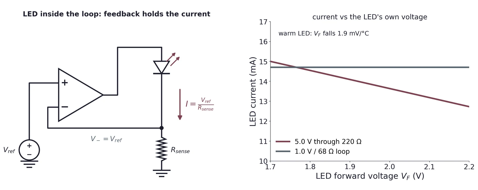
The op-amp output adjusts itself to , whatever happens to be. When the LED warms and drops, the output simply drops with it. Three limits bound the design and must all be checked:
- The output must stay inside its swing, even at the top of the knob: V.
- The LED current must stay within its rating (30 mA).
- The current must stay within the op-amp's own output limit (25 mA for the LM741), a common oversight.
For Task 1.2, the 5.0 V limit again applies to the node you call "the voltage applied to the LED" (§4.1). With the follower, that is the op-amp output. With the regulator, the output sits at , so bound both terms. Either way, name the node in your report and show that it cannot exceed 5.0 V.
(a) Explain in two sentences why the regulator of §6.2 holds its current steadier than a series resistor when the LED warms and falls by 0.1 V. Estimate the change for a 12 V source and a 470 Ω resistor.
(b) With from a pot between 0 and 2.0 V, choose so the LED current never exceeds 15 mA. What is the largest output voltage the op-amp must produce?
(c) A student uses = 22 Ω with up to 1.0 V. What limits the current, and what happens at the output?
7 The Photodiode
7.1 Light in, current out
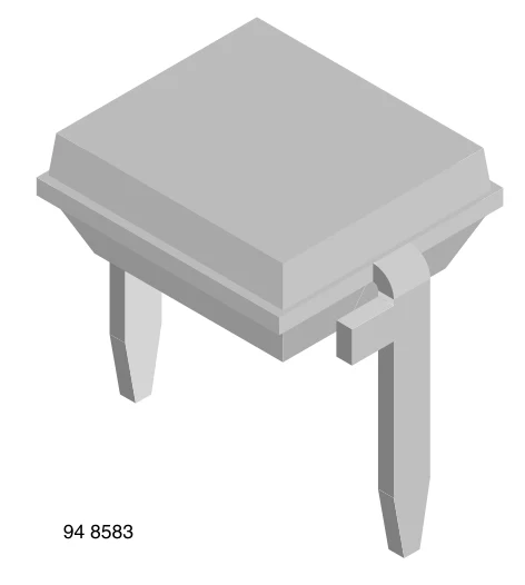
A photodiode is a PN (or PIN) junction built to let light into its depletion region. A photon with at least the band-gap energy creates an electron–hole pair; the junction's built-in field sweeps the electron to the N side and the hole to the P side. That flow of charge is a current, from cathode to anode inside the diode. This is the reverse of the direction current flows when a diode conducts normally.
7.2 The model
photodiode = a light-dependent current source inside an ordinary diode
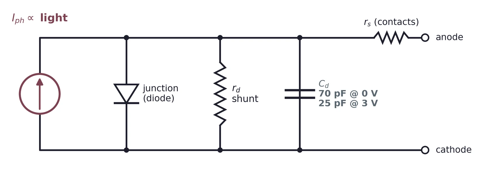
The terminal current is the diode's own current minus the photocurrent:
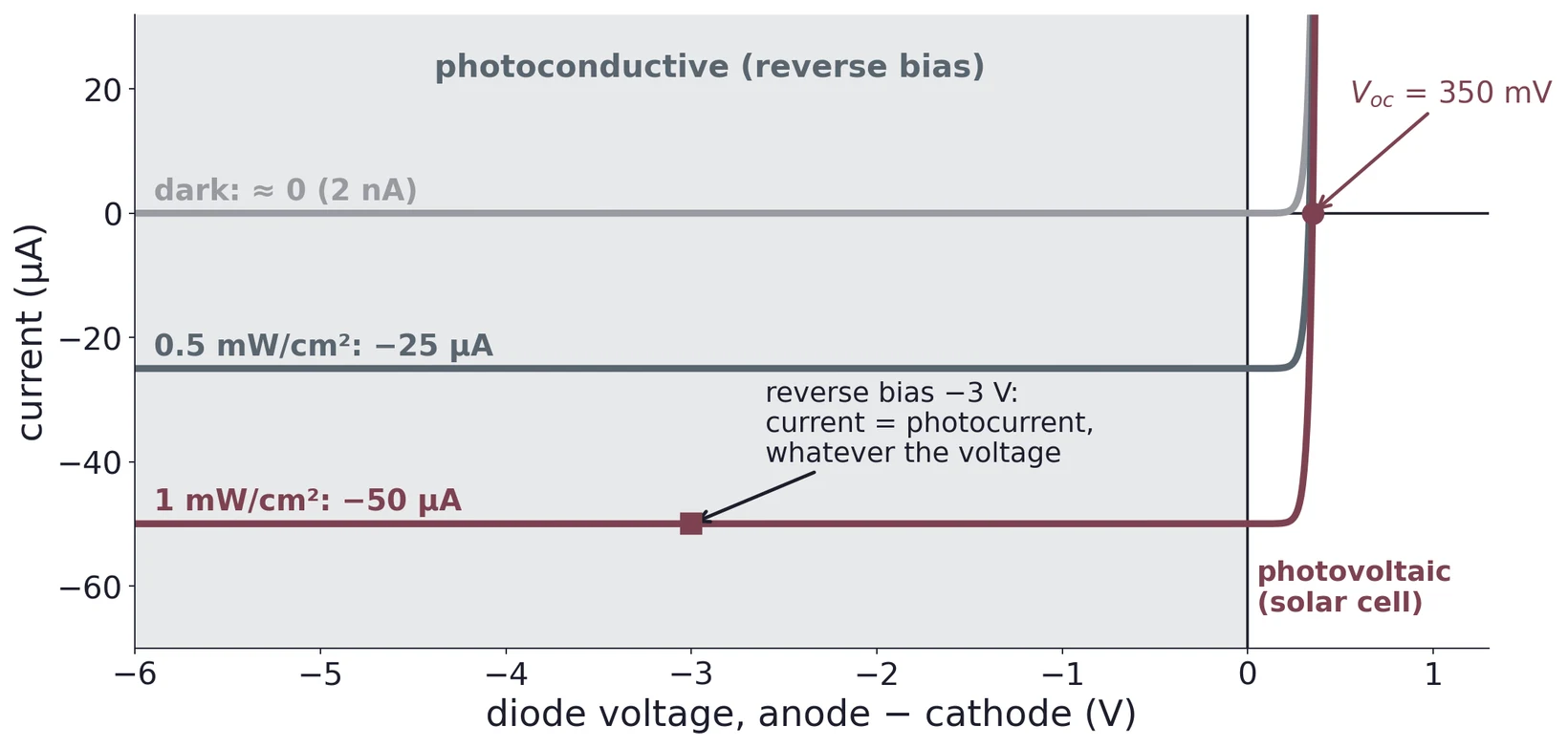
7.3 Light shifts the I–V curve down
| Operating mode | Bias | Behavior |
|---|---|---|
| Photovoltaic | zero bias | No bias-driven dark current, so the noise is low. But the junction capacitance is large and the detector is slow, and with a resistor load the response compresses near . |
| Photoconductive | reverse bias | The operating point sits on the flat part of the curve, so the current equals ; the wider depletion region lowers the capacitance and raises bandwidth. The cost is dark current. |
7.4 What the datasheet says
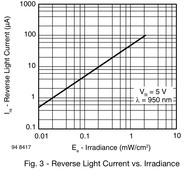
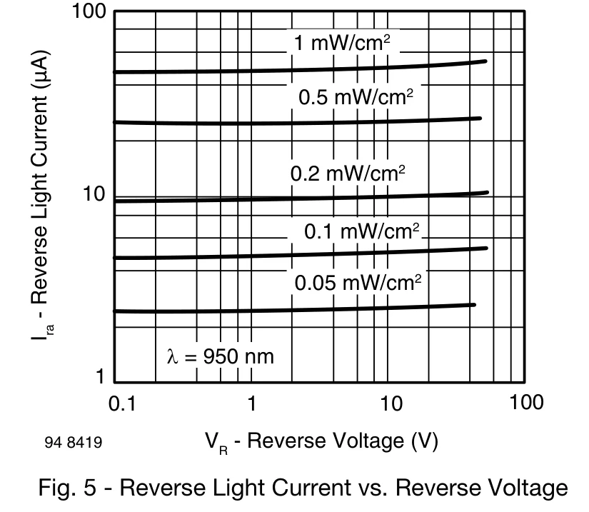
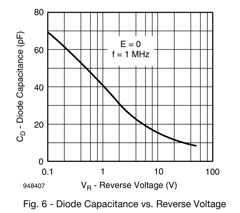
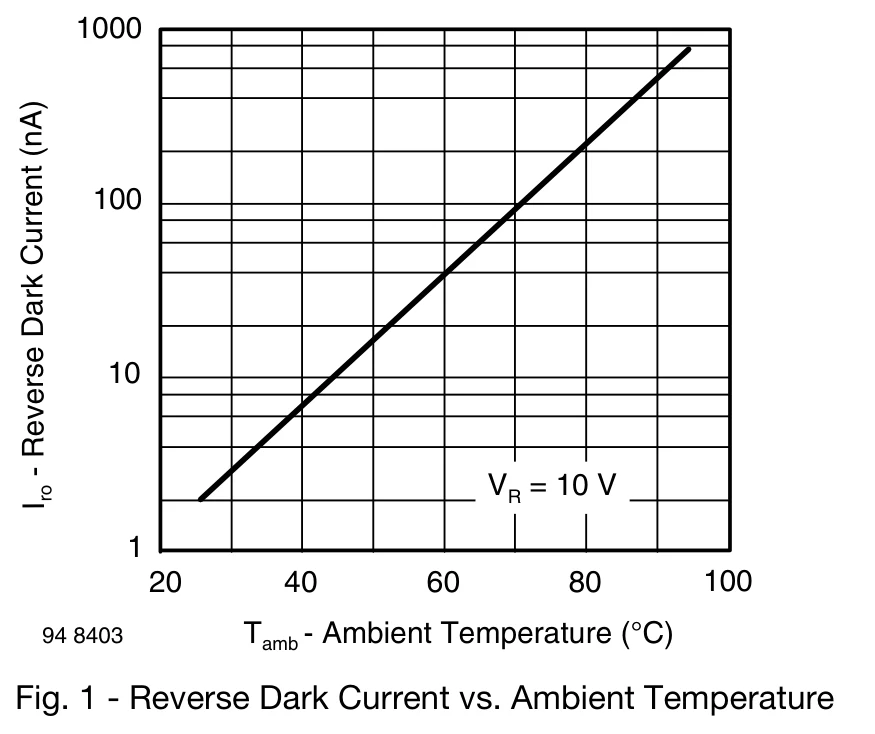
Dark current is the leakage that flows with no light, from thermally generated carriers and surface leakage. It grows with reverse voltage and, from Figure 20, rises about 400 times over 70 °C: a doubling roughly every 8 °C. In a detector it appears as an offset, and its shot noise, , sets part of the smallest signal you can detect. Subtracting a dark reading, or chopping the light, removes the offset.
8 The Resistor Detector
8.1 The circuit and its limit
The simplest detector puts the photodiode in reverse bias in series with a resistor . In Figure 21 the anode goes to −15 V and the cathode to node A, with from node A to ground. The photocurrent leaves node A into the diode, so current flows up from ground through and node A goes negative:
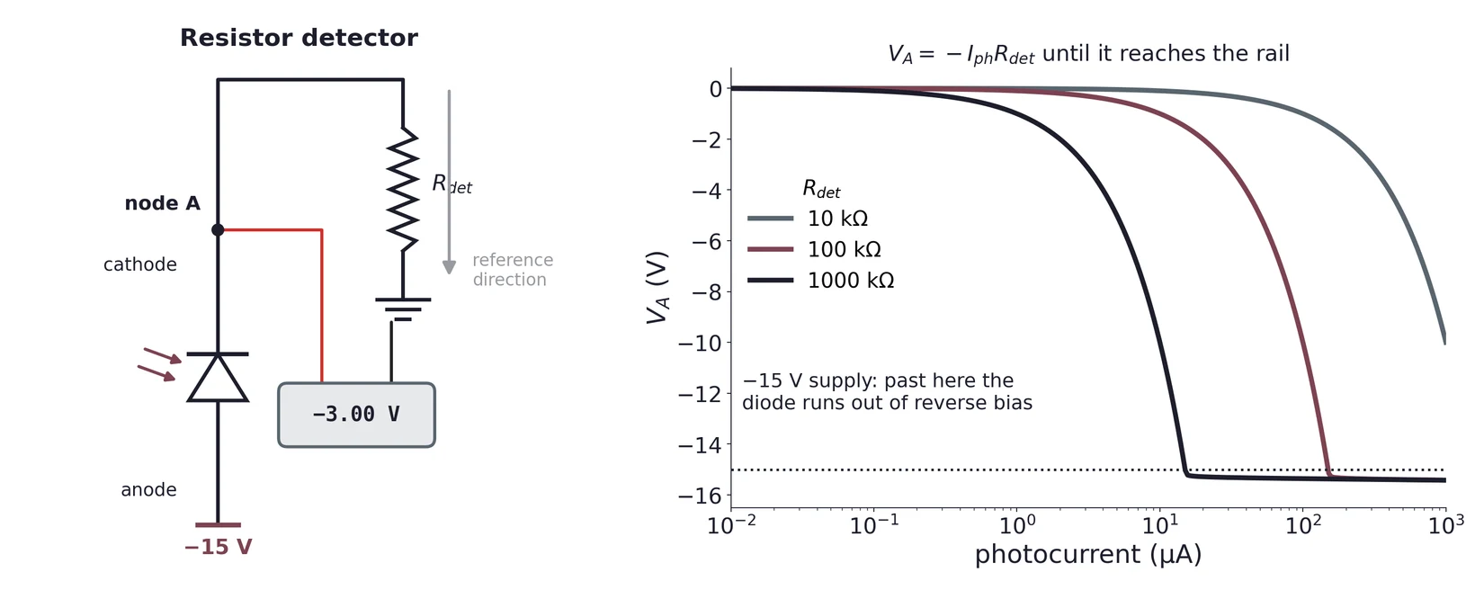
The resistor voltage appears across the diode too: the diode sees of reverse bias. A larger gives more volts per microamp, but it reaches the bias at a smaller photocurrent. It is also slower: the diode's capacitance charges through with time constant , and itself grows as the reverse bias shrinks. So one resistor sets the gain, the range and the speed, and you cannot adjust one without the others.
8.2 A negative reading is information
Task 2 asks for the current when the DMM reads −3.0 V. Define the voltage polarity and the current reference direction before doing any algebra. With the reference direction taken down through the detector resistor,
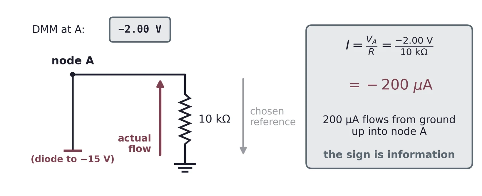
A negative value does not mean an arithmetic mistake, and it does not make the current imaginary. It means the true current flows opposite to the reference direction you chose. Write the convention in your report, in words or on the schematic, then quote the signed result and say what it means physically. " = −0.20 mA, i.e. 0.20 mA flowing from ground into node A" is a complete answer; "0.20 mA" alone is not. To get a positive reading you must turn the diode around and move its bias to +15 V (cathode to +15 V, anode to node A). Change only one of the two and the diode is forward biased, and it stops working as a detector.
Sanity-check the magnitude as well: 200 µA is a brightly lit BPW34 (extending the line of Figure 17 puts it near 4 mW/cm²), not a dim one.
(a) A 47 kΩ detector resistor reads −0.50 V. Find the current with its sign and describe its direction.
(b) Why might a 1 MΩ resistor be chosen over 10 kΩ, and what does it cost? Use Figure 21.
(c) A datasheet quotes 2 nA of dark current at 25 °C. Estimate it at 45 °C using the slope of Figure 20, and the offset it produces across 1 MΩ.
9 The Transimpedance Amplifier
9.1 The diode at virtual ground
A transimpedance amplifier (TIA) turns detector current straight into voltage. The photodiode connects to the inverting input, a feedback resistor runs from the output back to that input, and the non-inverting input is grounded. Rule 2 holds the inverting input at 0 V, a virtual ground. Rule 1 says the input takes no current, so all of the photocurrent must flow through .
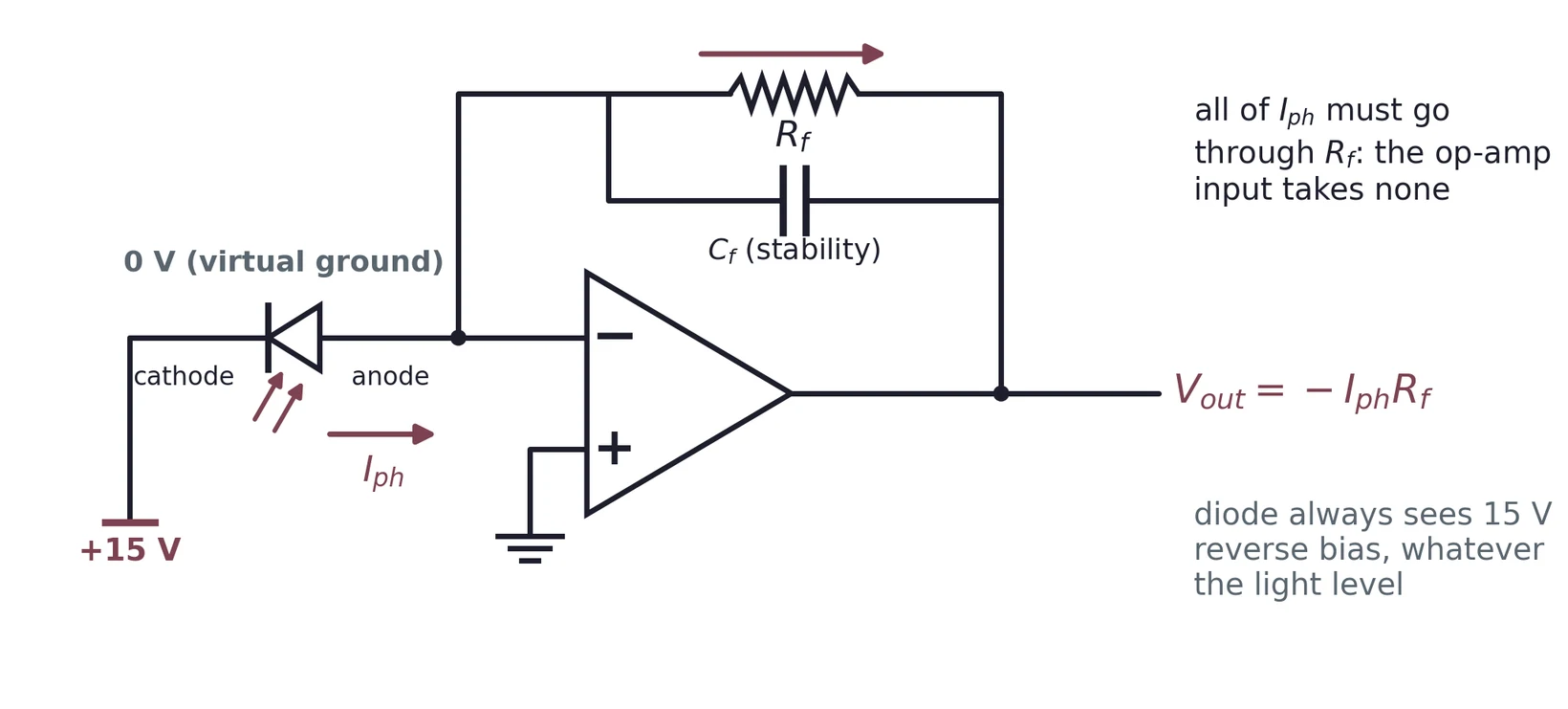
The minus sign comes from the direction of the current: it flows into the virtual-ground node, so the output must sit below 0 V to draw it through . Reverse the diode (anode to −15 V, cathode to the node) and the output goes positive.
9.2 Why the TIA beats the resistor
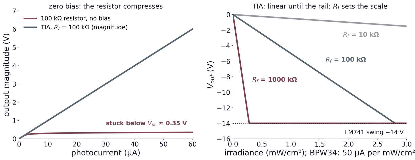
The resistor detector is simple and passive, but the voltage it develops appears across the diode and changes the very bias that makes it linear; gain, range and bandwidth are coupled through one resistor. The TIA sets the gain with and holds the photodiode at a fixed voltage, so the diode sees the same bias and the same capacitance at every light level. Pulling those apart is why the op-amp version is better.
9.3 Choosing R_f
The brightest light you expect must leave the output inside the rails:
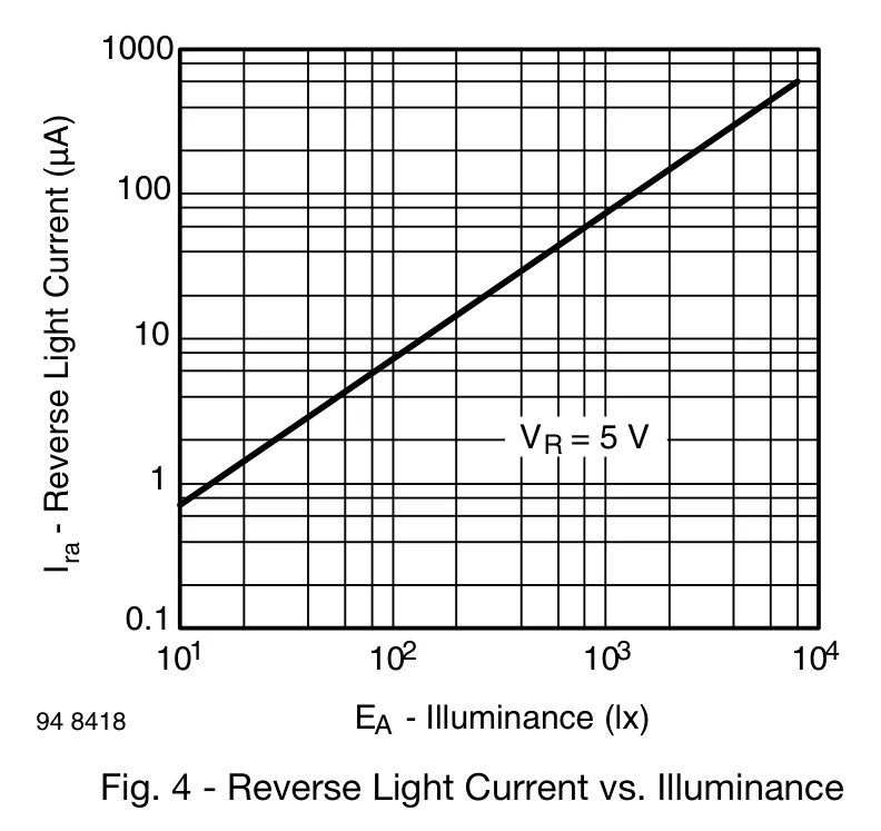
A photocurrent of 2 µA through = 100 kΩ gives V. Office lighting, about 500 lx, gives the BPW34 up to roughly 40 µA (Figure 25), or 4 V with the same resistor; the rail is reached at 140 µA. Treat the 40 µA as an upper guess. The datasheet measures its lux curve with an incandescent-type lamp (CIE illuminant A), which is rich in the near infrared where the BPW34 is most sensitive. White LED or fluorescent light of the same lux gives noticeably less current.
| V per µA | full scale at 14 V | |
|---|---|---|
| 10 kΩ | 0.01 V | 1.4 mA |
| 100 kΩ | 0.1 V | 140 µA |
| 1 MΩ | 1 V | 14 µA |
Measure your brightest case first, then choose the largest that still leaves headroom.
At high gain, remember that the op-amp's input bias current also flows through . For the LM741 (80 nA typical) and = 1 MΩ that puts about 80 mV on the output in total darkness, on top of the photodiode's own dark current. Cover the photodiode, record that dark reading, and subtract it.
9.4 Bandwidth and C_f
The detector capacitance sits between the inverting input and a fixed voltage. Together with it puts a pole in the feedback path, and the op-amp's own roll-off adds a second one. Two poles in the loop leave almost no phase margin, so the circuit rings, or even oscillates. If your TIA oscillates on the breadboard, this, not a wiring fault, is usually why. Without compensation the response peaks near
where is the op-amp's unity-gain frequency, about 1.2 MHz for the LM741. That comes from its 0.3 µs rise time using , the same rule the datasheet itself uses to quote bandwidth. A small capacitor across restores the phase margin; the usual choice for about 45° is
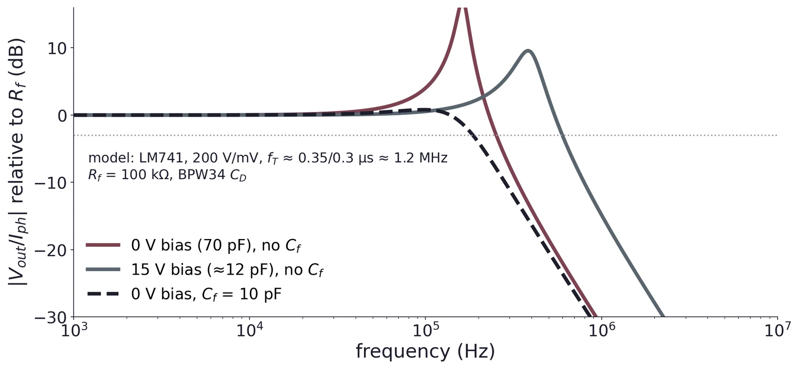
= 70 pF, = 100 kΩ, = 1.2 MHz. Equation (12) puts the uncompensated peak at kHz, and Equation (13) gives pF. The compensated corner, , is then about 160 kHz. Reverse bias lowers and pushes all of these up.
(a) The brightest light at your bench gives 25 µA. Choose a standard that keeps the LM741 at least 2 V inside its swing.
(b) With that and the BPW34 at 15 V bias (about 12 pF), estimate the from Equation (13) and the resulting bandwidth.
(c) Task 2.2 asks for the current when the output reads −3.0 V. Write the two facts you must state before you divide.
10 Lab 1 Task 3: Reading an Op-Amp Circuit
Task 3 gives you an op-amp circuit and asks for and , a sketch of , and over at least two periods, an explanation of each functional block, and a comparison with a SPICE simulation. The supply rails are ±15 V and is a 1 V-peak sine. (The manual calls the source V1; is the node it drives, so they are the same signal.)
10.1 Find the blocks first
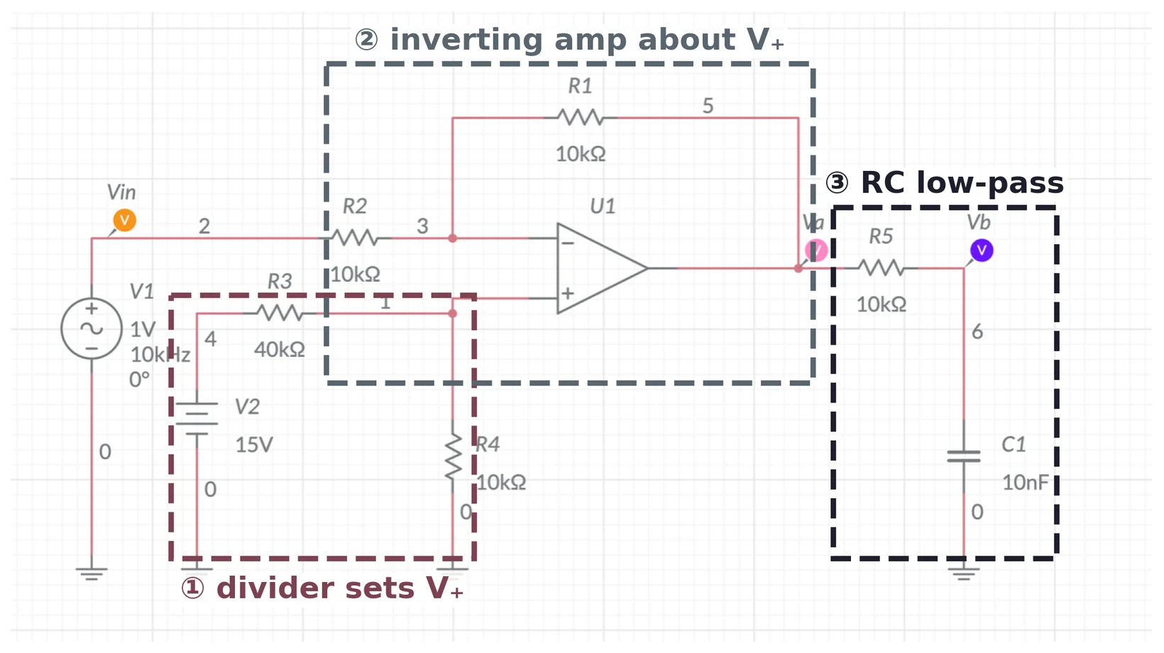
Naming the blocks is explicitly part of the task, and it is most of the work: each block is a circuit you can solve alone.
10.2 A biased inverting amplifier
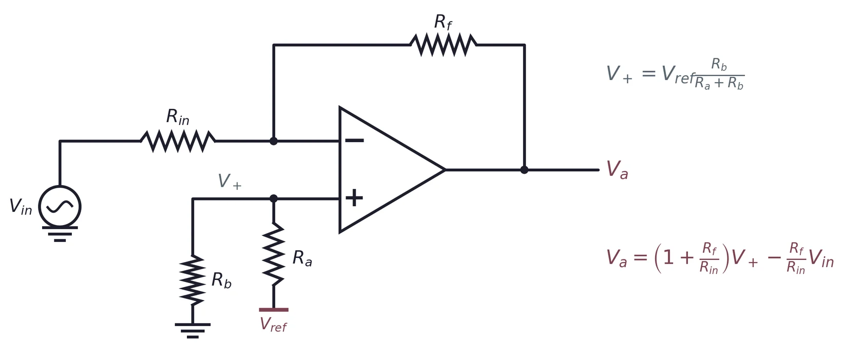
Solve it by superposition, one source at a time, using the two op-amp rules.
- alone ( = 0): the inverting input is a virtual ground; the current must flow on through , so .
- alone ( = 0): the inverting input follows , and , form a non-inverting amplifier, so .
The mistake to avoid is referring the inverting relation to ground: the DC level of is , not and not zero.
10.3 The RC low-pass
and form a first-order low-pass filter. At frequency , with ,
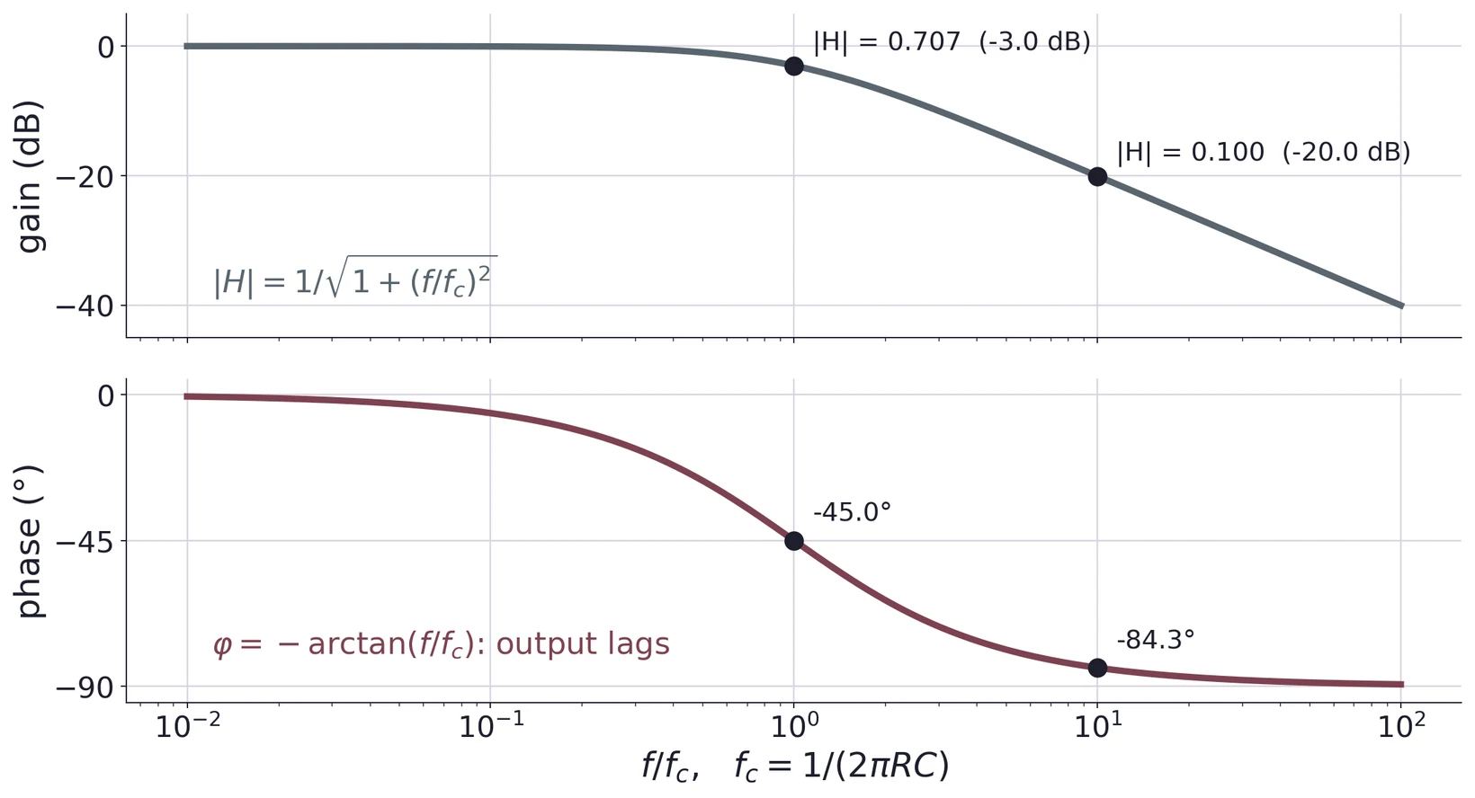
DC passes untouched, so keeps 's DC level; the sine is multiplied by and delayed by . A negative phase means the output lags. Show that lag in your sketch; two curves drawn exactly in phase show the phase was never computed. Check also that nothing disturbs the filter. The op-amp output drives with almost no source resistance, and drives only the probe, so Equation (15) applies as it stands.
10.4 Worked example with other values
Take = 12 V with = 30 kΩ and = 10 kΩ, so V; = 2; and an RC filter of 10 kΩ and 47 nF, with a 1 V, 1 kHz sine.
- Equation (14): V, swinging from 7 to 11 V, inverted.
- Hz, so = 2.95.
- Equation (15): and .
- V.
- Every voltage stays between 7 and 11 V, well inside ±15 V, so nothing clips.
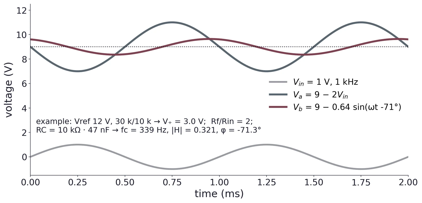
Carry symbols as far as you can before substituting numbers, so the structure of the answer stays visible. Quote and as explicit functions of time with amplitude, DC level and phase. Draw all three traces on one set of axes with a labeled voltage scale, so the gain and the offset can be read off. Then overlay the simulation result and comment on any difference: a small discrepancy traced to a real cause is worth more than a perfect match asserted without checking.
11 Common Mistakes and Bench Safety
- LED backwards. It will not light, and across more than 5 V it may be damaged. Long lead to the positive side.
- No series resistance. A follower set to 5 V with no tries to push far more than 30 mA into the LED. Only the op-amp's own short-circuit limit (25 mA typical, not guaranteed) holds it back, and the op-amp runs hot. That limit is a safety net, not a design feature.
- Supplies on the wrong pins. LM741 pin 7 is +15 V and pin 4 is −15 V; reversing them destroys the part. Check the notch before powering on.
- Floating non-inverting input. Ground it (TIA) or connect it to its divider; a floating input makes the output wander to a rail.
- Oscillating TIA. A fuzzy or ringing output on the scope with no light change is the capacitance problem of §9.4. Add .
- Wrong DMM polarity. Note which lead is on which node before you read. The sign is part of the answer.
12 Self-Check
- Why is an LED an unsafe load for a voltage source, and what does a series resistor change about that?
- State the two separate requirements in Task 1.1 and the calculation each one demands.
- Why does a 7 kΩ / 5 kΩ divider fail to drive an LED, and how does a follower fix it?
- In the current regulator of §6.2, what sets the current, and what three limits must be checked?
- A detector resistor reads −0.80 V across 22 kΩ. What is the current under the stated reference direction, and what does the sign mean physically?
- Give two advantages of reverse-biasing a photodiode, and the price.
- Why does a TIA produce ? Where does the minus sign come from, and what holds the input at virtual ground?
- What limits a TIA's bandwidth, and what does do?
- Name the three functional blocks in the Task 3 circuit and state what each contributes to .
- What two numbers describe what an RC low-pass does to a sine, and how do you show each on the sketch?
13 Practical Engineering Connections
- LED drivers. Current limiting appears in status indicators, infrared remote controls, barcode scanners, optical encoders and fiber-optic transmitters. Constant-current regulators like §6.2 drive nearly every LED lamp and backlight, because brightness follows current.
- Photodiode detectors. A photodiode and resistor form the front end of light meters, smoke detectors, automatic brightness controls, optical interrupters and IR receivers.
- Transimpedance amplifiers. TIAs appear in fiber-optic receivers, laser-power monitors, pulse oximeters, imaging sensors and optical links, anywhere a small detector current must become a low-noise voltage. Their bandwidth-versus-capacitance trade-off is the central problem of optical receiver design.
- Biased amplifier plus RC filter. The Task 3 chain is a basic sensor-conditioning circuit: shift the level, set the range, limit the bandwidth, prepare the signal for an ADC. You will meet the digital half of this chain in Lab 8.
- System-level design. A real product combines current limiting, biasing, feedback, filtering, supply decoupling, calibration and protection. Getting the equation right is only part of the job, and that idea runs through the whole course.