Due: 2:00 p.m. before your next lab section.
- Lab Log: Keep a complete lab log: circuit diagrams, measurements, analysis steps, and observations. Include clear photographs of instrument readings and circuit setups.
- Report Format: Submit a typed lab report in PDF format. Hand-drawn circuit diagrams will not be accepted; draw every schematic with software (see Software at the end of this manual).
- Time: Plan your time. Makeup sessions are available by appointment with your TA, subject to their availability.
- AI Policy: The use of any AI tool, including a large language model (LLM), to write, generate, debug, or modify code or any portion of the lab report is prohibited unless the course instructor grants explicit permission in advance. A teaching assistant (TA) cannot grant permission to use AI tools.
By signing below, I acknowledge that I have read and understood the policies and instructions above and agree to follow them.
Student Name (print):
Student Signature: Date:
All tasks in this lab are required. The Lecture 06 notes cover the methods you need.
Task 1: Transistor Characterization
Using a digital multimeter (DMM), measure the pin-to-pin characteristics of the transistors (2N3904 and 2N3906) to verify their configuration. Record your measurements in the table below.
| + | − | 2N3904 | 2N3906 |
|---|---|---|---|
| B | C | ||
| B | E | ||
| C | E | ||
| C | B | ||
| E | B | ||
| E | C |
Course Instructor or TA Signature:
Date and Time:
Task 2: Voltage Divider Bias Circuit Design
Based on your measurements from Task 1, design and construct a voltage divider bias circuit for the 2N3904 transistor. Use the following parameters:
- Unadjustable V,
- All resistors must be greater than 300 Ω,
- The voltage divider should satisfy: ,
- The current through : , preferably ,
- Target emitter voltage: ,
- Desired collector-emitter voltage: .
Measure and record the following:
Calculate the transistor's current gain using your measurements and compare it with the datasheet value, ensuring that the transistor operates in the active region (i.e., it is not saturated).
Course Instructor or TA Signature:
Date and Time:
Task 3: CE Amplifier Construction and AC Signal Analysis
Use the bias network from Task 2 to build a common-emitter amplifier (Figure 1). First, generate an AC signal with:
- Peak-to-peak voltage mV,
- Frequency between 2 kHz and 20 kHz.
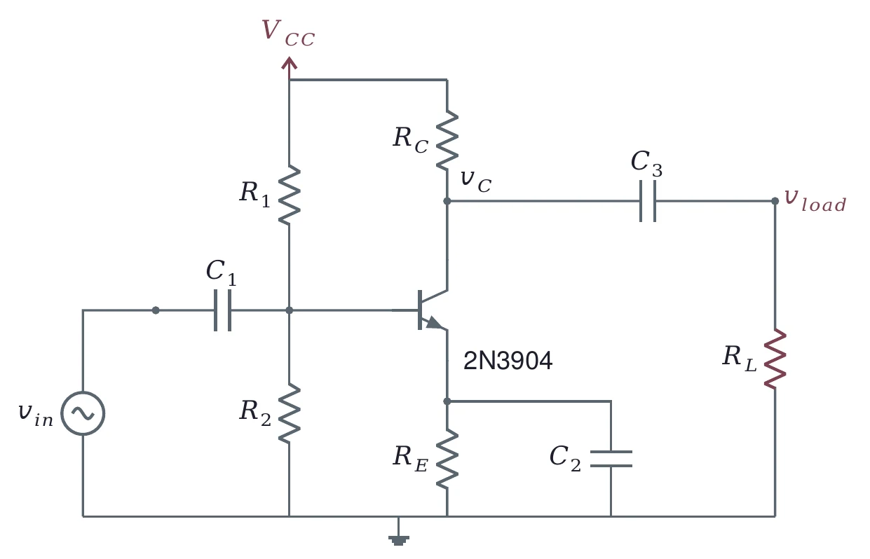
Apply this signal as the input to your amplifier circuit. Measure and record the following:
- The output waveform's amplitude,
- The DC offset,
- The phase shift relative to the input.
Additionally, measure the open-load AC voltage gain , which should exceed 40.
Course Instructor or TA Signature:
Date and Time:
Task 4: Amplifier Load Testing
Evaluate the amplifier's performance under various load conditions. Connect a coupling capacitor and perform the following:
- Attach a 10 kΩ load resistor to the amplifier's output and record the loaded AC voltage gain .
- Using a third BNC cable, simultaneously display the input (), collector (), and loaded output () waveforms on the oscilloscope.
- Repeat the measurement with 2 kΩ and 300 Ω load resistors.
- Explain any observed variations in gain and waveform characteristics as the load resistance changes.
Course Instructor or TA Signature:
Date and Time:
Submission Reminder
- Your lab log notes and photographs of the instrument readings and the circuits.
- Task 1: the completed pin measurement table for both transistors.
- Task 2: the schematic with your resistor values, your design calculations, every measured current and voltage, and compared with the datasheet value.
- Task 3: the schematic with your capacitor values, the output amplitude, DC offset and phase shift, and the open-load gain .
- Task 4: the loaded gain for each load, the three-channel captures, and your explanation of the changes.
- An error analysis for every task where it applies: the uncertainty of each measured or calculated value, its main sources of error, and a comparison with the expected, simulated, or datasheet value.
- A discussion of any challenges you met and how you solved them.
Draw every circuit diagram with software; hand-drawn circuit diagrams will not be accepted. We recommend the free draw.io; the course’s Drawing Circuit Diagrams page shows how to set it up. If a component has no symbol of its own, use the closest one and label it clearly.
Where a task asks for a simulation: the web version of Multisim is no longer available. If you have a Windows computer, you can install the offline (desktop) version of Multisim; ask a TA for the serial number to install it. Otherwise, feel free to use any SPICE-based simulation tool, such as LTspice or ngspice.